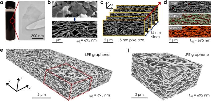
БЛОГ

Archive for the ‘nanotechnology’ category: Page 127

Oct 7, 2020

“World’s fastest electrodes” triple the density of lithium batteries

Posted by in categories: energy, nanotechnology

French company Nawa technologies says it’s already in production on a new electrode design that can radically boost the performance of existing and future battery chemistries, delivering up to 3x the energy density, 10x the power, vastly faster charging and battery lifespans up to five times as long.

Nawa is already known for its work in the ultracapacitor market, and the company has announced that the same high-tech electrodes it uses on those ultracapacitors can be adapted for current-gen lithium-ion batteries, among others, to realize some tremendous, game-changing benefits.

Continue reading “‘World’s fastest electrodes’ triple the density of lithium batteries” »

Oct 5, 2020

Inflight fiber printing toward array and 3D optoelectronic and sensing architectures

Posted by in categories: 3D printing, chemistry, nanotechnology, wearables

Scalability and device integration have been prevailing issues limiting our ability in harnessing the potential of small-diameter conducting fibers. We report inflight fiber printing (iFP), a one-step process that integrates conducting fiber production and fiber-to-circuit connection. Inorganic (silver) or organic {PEDOT: PSS [poly(3,4-ethylenedioxythiophene) polystyrene sulfonate]} fibers with 1- to 3-μm diameters are fabricated, with the fiber arrays exhibiting more than 95% transmittance (350 to 750 nm). The high surface area–to–volume ratio, permissiveness, and transparency of the fiber arrays were exploited to construct sensing and optoelectronic architectures. We show the PEDOT: PSS fibers as a cell-interfaced impedimetric sensor, a three-dimensional (3D) moisture flow sensor, and noncontact, wearable/portable respiratory sensors. The capability to design suspended fibers, networks of homo cross-junctions and hetero cross-junctions, and coupling iFP fibers with 3D-printed parts paves the way to additive manufacturing of fiber-based 3D devices with multilatitude functions and superior spatiotemporal resolution, beyond conventional film-based device architectures.

Small-diameter conducting fibers have unique morphological, mechanical, and optical properties such as high aspect ratio, low bending stiffness, directionality, and transparency that set them apart from other classes of conducting, film-based micro/nano structures (1–3). Orderly assembling of thin conducting fibers into an array or three-dimensional (3D) structures upscales their functional performance for device coupling. Developing new strategies to control rapid synthesis, patterning, and integration of these conducting elements into a device architecture could mark an important step in enabling new device functions and electronic designs (4, 5). To date, conducting micro/nanoscaled fibers have been produced and assembled in a number of ways, from transferring of chemically grown nanofibers/wires (6, 7), writing electrohydrodynamically deposited lines (8, 9), to drawing ultralong fibers (10, 11), wet spinning of fibers (12–14), and 2D/3D direct printing (15–18).

Oct 4, 2020

A new technique for the production of plasmonics devices

Posted by in categories: nanotechnology, particle physics

Research laboratories are constantly developing new materials that are expected to exhibit novel properties bound to revolutionize this or that technology. But it’s not enough to simply create these materials; scientists also need to find efficient methods of processing and fine-tuning them.

Moreover, composites are often made via the addition of nanoparticles into a base matrix, which is why it is necessary to find a way of manipulating the location, size, and concentration rate of these particles that would exclude even the smallest deviations that are invisible to the human eye.

Researchers from ITMO University have improved on the technique of local processing of composites based on nanoporous glass with addition of silver and copper. Now, it is possible to predict with high accuracy the optical properties of a plasmonic component during its treatment.

Oct 3, 2020

The Road to Human 2.0

Posted by in categories: 3D printing, biotech/medical, computing, genetics, life extension, nanotechnology, neuroscience, transhumanism

In the coming 2020s, the world of medical science will make some significant breakthroughs. Through brain implants, we will have the capability to restore lost memories.

~ The 2020s will provide us with the computer power to make the first complete human brain simulation. Exponential growth in computation and data will make it possible to form accurate models of every part of the human brain and its 100 billion neurons.

~ The prototype of the human heart was 3D printed in 2019. By the mid- 2020s, customized 3D- printing of major human body organs will become possible. In the coming decades, more and more of the 78 organs in the human body will become printable.

Continue reading “The Road to Human 2.0” »

Oct 2, 2020

Radiation-immune and repairable chips to fabricate durable electronics

Posted by in categories: computing, nanotechnology

To operate safely and reliably in outdoor environments, electronic devices should be resistant to a wide variety of external factors, including radiation. In fact, high-energy radiation can damage several components of field-effect transistors (FETs) commonly used to make electronics, including their superconducting channel, gate oxide and the insulating materials surrounding it (e.g., isolation or substrate oxides).

For several years, research teams worldwide have thus been trying to devise strategies that could make more resistant to radiation. So far, however, this has proved to be highly challenging, and only a few of the techniques proposed in the past have achieved promising results.

Researchers at Peking University, the Chinese Academy of Sciences and Shanghai Tech University have recently fabricated a radiation-hardened and repairable integrated circuit (IC) based on carbon nanotube transistors with ion gel . This IC, first presented in a paper pre-published in Nature Electronics, could be used to build new that are more resistant to high-energy radiation.

Oct 2, 2020

New nanotechology design provides hope for personalized vaccination for treating cancer

Posted by in categories: biotech/medical, chemistry, nanotechnology

One of the key challenges in developing effective, targeted cancer treatments is the heterogeneity of the cancer cells themselves. This variation makes it difficult for the immune system to recognize, respond to and actively fight against tumors. Now, however, new advances in nanotechnology are making it possible to deliver targeted, personalized “vaccines” to treat cancer.

A new study, published on October 2, 2020 in Science Advances, demonstrates the use of charged nanoscale metal-organic frameworks for generating free radicals using X-rays within tumor tissue to kill directly. Furthermore, the same frameworks can be used for delivering immune signaling molecules known as PAMPs to activate the immune response against . By combining these two approaches into one easily administered “vaccine,” this new technology may provide the key to better local and systemic treatment of difficult-to-treat cancers.

In a collaboration between the Lin Group in the University of Chicago Department of Chemistry and the Weichselbaum Lab at University of Chicago Medicine, the research team combined expertise from inorganic chemistry and to tackle the challenging problem of properly targeting and activating an innate immune response against . This work leveraged the unique properties of nanoscale metal-organic frameworks, or nMOFs —nanoscale structures built of repeating units in a lattice formation that are capable of infiltrating tumors.

Oct 2, 2020

Tunable free-electron X-ray radiation from van der Waals materials

Posted by in categories: biotech/medical, chemistry, engineering, nanotechnology, quantum physics, security

Technion researchers have developed accurate radiation sources that are expected to lead to breakthroughs in medical imaging and other areas. They have developed precise radiation sources that may replace the expensive and cumbersome facilities currently used for such tasks. The suggested apparatus produces controlled radiation with a narrow spectrum that can be tuned with high resolution, at a relatively low energy investment. The findings are likely to lead to breakthroughs in a variety of fields, including the analysis of chemicals and biological materials, medical imaging, X-ray equipment for security screening, and other uses of accurate X-ray sources.

Published in the journal Nature Photonics, the study was led by Professor Ido Kaminer and his master’s student Michael Shentcis as part of a collaboration with several research institutes at the Technion: the Andrew and Erna Viterbi Faculty of Electrical Engineering, the Solid State Institute, the Russell Berrie Nanotechnology Institute (RBNI), and the Helen Diller Center for Quantum Science, Matter and Engineering.

The researchers’ paper shows an experimental observation that provides the first proof-of-concept for theoretical models developed over the last decade in a series of constitutive articles. The first article on the subject also appeared in Nature Photonics. Written by Prof. Kaminer during his postdoc at MIT, under the supervision of Prof. Marin Soljacic and Prof. John Joannopoulos, that paper presented theoretically how two-dimensional materials can create X-rays. According to Prof. Kaminer, “that article marked the beginning of a journey towards sources based on the unique physics of two-dimensional materials and their various combinations—heterostructures. We have built on the theoretical breakthrough from that article to develop a series of follow-up articles, and now, we are excited to announce the first experimental observation on the creation of X-ray radiation from such materials, while precisely controlling the radiation parameters.”

Oct 1, 2020

E-beam atomic-scale 3D ‘sculpting’ could enable new quantum nanodevices

Posted by in categories: engineering, nanotechnology, quantum physics

Based on focused -induced processing (FEBID) techniques, the work could allow production of 2-D/3D complex nanostructures and functional nanodevices useful in quantum communications, sensing, and other applications. For oxygen-containing materials such as graphene oxide, etching can be done without introducing outside materials, using oxygen from the substrate.

“By timing and tuning the energy of the electron , we can activate interaction of the beam with oxygen in the graphene oxide to do etching, or interaction with hydrocarbons on the surface to create carbon deposition,” said Andrei Fedorov, professor and Rae S. and Frank H. Neely Chair in the George W. Woodruff School of Mechanical Engineering at the Georgia Institute of Technology. “With atomic-scale control, we can produce complicated patterns using direct write-remove processes. Quantum systems require precise control on an atomic scale, and this could enable a host of potential applications.”

Sep 29, 2020

Why disordered light-harvesting systems produce ordered outcomes

Posted by in categories: chemistry, energy, nanotechnology, physics

Scientists typically prefer to work with ordered systems. However, a diverse team of physicists and biophysicists from the University of Groningen found that individual light-harvesting nanotubes with disordered molecular structures still transport light energy in the same way. By combining spectroscopy, molecular dynamics simulations and theoretical physics, they discovered how disorder at the molecular level is effectively averaged out at the microscopic scale. The results were published on 28 September in the Journal of the American Chemical Society.

The double-walled light-harvesting nanotubes self-assemble from molecular building blocks. They are inspired by the multi-walled tubular antenna network of photosynthetic bacteria found in nature. The nanotubes absorb and transport light energy, although it was not entirely clear how. “The nanotubes have similar sizes but they are all different at the with the molecules arranged in a disordered way,” explains Maxim Pshenichnikov, Professor of Ultrafast Spectroscopy at the University of Groningen.

Sep 26, 2020

Physicists Play With the Laws of Nature: Controlling Ultrastrong Light-Matter Coupling at Room Temperature

Posted by in categories: chemistry, nanotechnology, quantum physics

Physicists at Chalmers, together with colleagues in Russia and Poland, have managed to achieve ultrastrong coupling between light and matter at room temperature. The discovery is of importance for fundamental research and might pave the way for advances within, for example, light sources, nanomachinery, and quantum technology.

A set of two coupled oscillators is one of the most fundamental and abundant systems in physics. It is a very general toy model that describes a plethora of systems ranging from guitar strings, acoustic resonators, and the physics of children’s swings, to molecules and chemical reactions, from gravitationally bound systems to quantum cavity electrodynamics. The degree of coupling between the two oscillators is an important parameter that mostly determines the behavior of the coupled system. However, the question is rarely asked about the upper limit by which two pendula can couple to each other – and what consequences such coupling can have.

The newly presented results, published in Nature Communications, offer a glimpse into the domain of the so-called ultrastrong coupling, wherein the coupling strength becomes comparable to the resonant frequency of the oscillators. The coupling in this work is realized through interaction between light and electrons in a tiny system consisting of two gold mirrors separated by a small distance and plasmonic gold nanorods. On a surface that is a hundred times smaller than the end of a human hair, the researchers have shown that it is possible to create controllable ultrastrong interaction between light and matter at ambient conditions – that is, at room temperature and atmospheric pressure.