Nano bots.
Nano Robotics is revolutionizing the manufacturing industry. It combines nanotechnology, robotics, and artificial intelligence to produce highly efficient and precise machines.


On the highway of heat transfer, thermal energy is moved by way of quantum particles called phonons. But at the nanoscale of today’s most cutting-edge semiconductors, those phonons don’t remove enough heat. That’s why Purdue University researchers are focused on opening a new nanoscale lane on the heat transfer highway by using hybrid quasiparticles called “polaritons.”
Thomas Beechem loves heat transfer. He talks about it loud and proud, like a preacher at a big tent revival.
“We have several ways of describing energy,” said Beechem, associate professor of mechanical engineering. “When we talk about light, we describe it in terms of particles called ‘photons.’ Heat also carries energy in predictable ways, and we describe those waves of energy as ‘phonons.’ But sometimes, depending on the material, photons and phonons will come together and make something new called a ‘polariton.’ It carries energy in its own way, distinct from both photons or phonons.”

In the era of big data and advanced artificial intelligence, traditional data storage methods are becoming inadequate. To address the need for high-capacity and energy-efficient storage solutions, the development of next-generation technologies is crucial.
Among these is resistive random-access memory (RRAM), which relies on altering resistance levels to store data. A recent study published in the journal Angewandte Chemie details the work of a research team who have pioneered a method for creating supramolecular memristors, one of the key components in the construction of nano-RRAM.

With a hydrogen production rate of 139 millimoles per hour and per gram of catalyst, the material holds the world record for green hydrogen production with sunlight.
Scharfsinn86/iStock.
Professor Emiliano Cortés, a leading figure in experimental physics and energy conversion at LMU, and Dr. Matías Herrán, a postdoc researcher at the Fritz Haber Institute of the Max Planck Society, delved into the intricate world of nanotechnology to develop high-performance nanostructures that could revolutionize solar energy utilization.
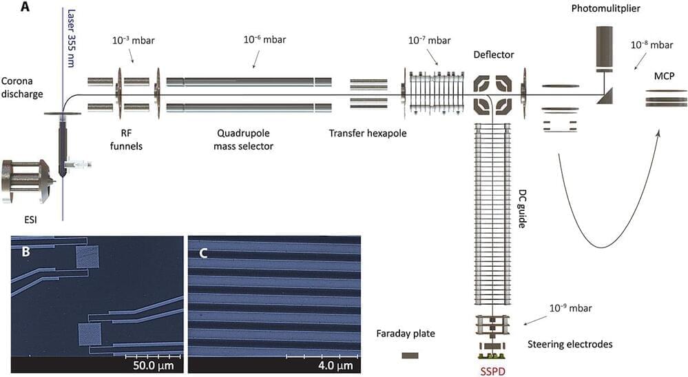
An international research team led by quantum physicist Markus Arndt (University of Vienna) has achieved a breakthrough in the detection of protein ions: Due to their high energy sensitivity, superconducting nanowire detectors achieve almost 100% quantum efficiency and exceed the detection efficiency of conventional ion detectors at low energies by a factor of up to a 1,000.
In contrast to conventional detectors, they can also distinguish macromolecules by their impact energy. This allows for more sensitive detection of proteins and it provides additional information in mass spectrometry.
A researcher has just finished writing a scientific paper. She knows her work could benefit from another perspective. Did she overlook something? Or perhaps there’s an application of her research she hadn’t thought of. A second set of eyes would be great, but even the friendliest of collaborators might not be able to spare the time to read all the required background publications to catch up.
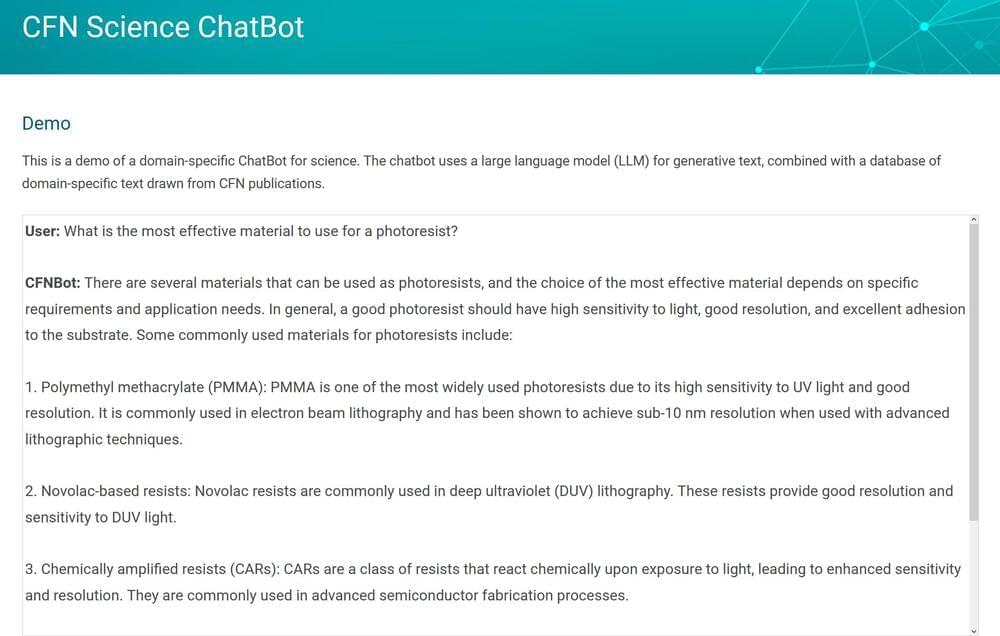
Kevin Yager—leader of the electronic nanomaterials group at the Center for Functional Nanomaterials (CFN), a U.S. Department of Energy (DOE) Office of Science User Facility at DOE’s Brookhaven National Laboratory—has imagined how recent advances in artificial intelligence (AI) and machine learning (ML) could aid scientific brainstorming and ideation. To accomplish this, he has developed a chatbot with knowledge in the kinds of science he’s been engaged in.
Rapid advances in AI and ML have given way to programs that can generate creative text and useful software code. These general-purpose chatbots have recently captured the public imagination. Existing chatbots—based on large, diverse language models—lack detailed knowledge of scientific sub-domains. By leveraging a document-retrieval method, Yager’s bot is knowledgeable in areas of nanomaterial science that other bots are not.
A research group has made new insights into how locomotion occurs in bacteria. The group identified the FliG molecule in the flagellar layer, the ‘motor’ of bacteria, and revealed its role in the organism. These findings suggest ways in which future engineers could build nanomachines with full control over their movements.
The researchers, who were led by Professor Emeritus Michio Homma and Professor Seiji Kojima of the Graduate School of Science at Nagoya University, in collaboration with Osaka University and Nagahama Institute of Bio-Science and Technology, published the study in iScience.
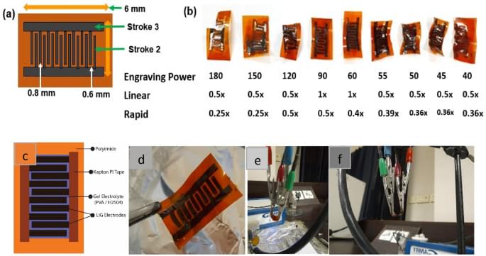
The field of supercapacitors consistently focuses on research and challenges to improve energy efficiency, capacitance, flexibility, and stability. Low-cost laser-induced graphene (LIG) offers a promising alternative to commercially available graphene for next-generation wearable and portable devices, thanks to its remarkable specific surface area, excellent mechanical flexibility, and exceptional electrical properties. We report on the development of LIG-based flexible supercapacitors with optimized geometries, which demonstrate high capacitance and energy density while maintaining flexibility and stability. Three-dimensional porous graphene films were synthesized, and devices with optimized parameters were fabricated and tested. One type of device utilized LIG, while two other types were fabricated on LIG by coating multi-walled carbon nanotubes (MWCNT) at varying concentrations.
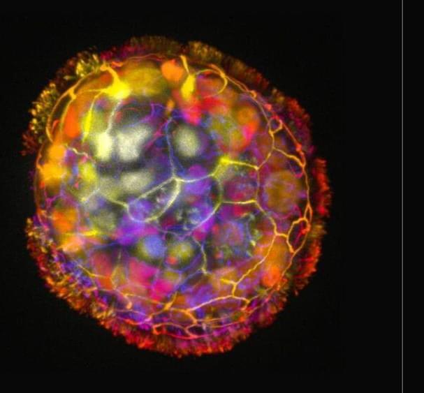
The researchers are excited by the potential of how cells cooperate and communicate in the body and how they can be reprogrammed to create new structures and functions.
With the help of Simon Garnier at the New Jersey Institute of Technology, the team characterized the different types of Anthrobots that were produced.
They observed that bots fell into a few discrete categories of shape and movement, ranging in size from 30 to 500 micrometers (from the thickness of a human hair to the point of a sharpened pencil), filling an important niche between nanotechnology and larger engineered devices.
Some were spherical and fully covered in cilia, and some were irregular or football-shaped with more patchy coverage of cilia or just covered with cilia on one side. They traveled in straight lines, moved in tight circles, combined those movements, or just sat around and wiggled.