БЛОГ

Archive for the ‘nanotechnology’ category: Page 159

Sep 13, 2019

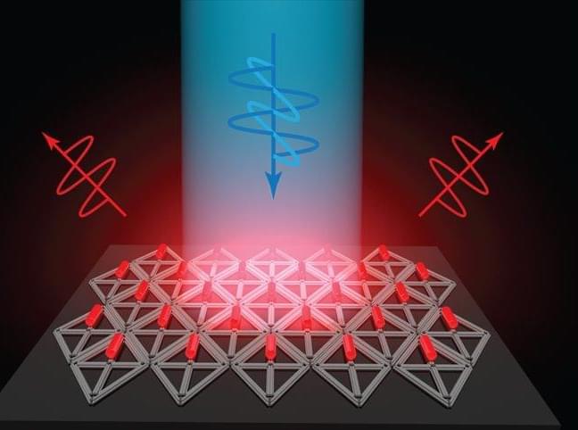
Scientists create a nanomaterial that is both twisted and untwisted at the same time

Posted by in categories: food, nanotechnology

A new nanomaterial developed by scientists at the University of Bath could solve a conundrum faced by scientists probing some of the most promising types of future pharmaceuticals.

Scientists who study the nanoscale—with molecules and materials 10,000 smaller than a pinhead—need to be able to test the way that some molecules twist, known as their , because mirror image molecules with the same structure can have very different properties. For instance one kind of molecule smells of lemons when it twists in one direction, and oranges when twisted the other way.

Detecting these twists is especially important in some high-value industries such as pharmaceuticals, perfumes, food additives and pesticides.

Sep 12, 2019

Dynamic charge density fluctuations pervading the phase diagram of a Cu-based high-Tc superconductor

Posted by in categories: energy, nanotechnology, quantum physics

Charge density fluctuations are observed in all families of high-critical temperature (Tc) superconducting cuprates. Although constantly found in the underdoped region of the phase diagram at relatively low temperatures, physicists are unclear how the substrates influence unusual properties of these systems. In a new study now published on Science, R. Arpaia and co-workers in the departments of microtechnology and nanoscience, the European Synchrotron, and quantum device physics in Italy, Sweden and France used resonant X-ray scattering to carefully determine the charge density modulations in Yttrium Barium Copper Oxide (YBa2Cu3O7– ẟ) and Neodymium Barium Copper Oxide (Nd1+x Ba2–x Cu3O7–ẟ) for several doping levels. The research team isolated short-range dynamic charge density fluctuations (CDFs) in addition to the previously known quasi-critical charge density waves (CDW). The results persisted well above the pseudo-gap temperature T*, which they characterized by a few milli-electron volts (meV) to spread across a large area of the phase diagram.

Cuprate high temperature superconductors (HTS) are different from the Landau Fermi liquid paradigm due to quasi-two dimensionality (2-D) of their layered structure and large electron-electron repulsion. During optimal doping and the pseudo gap state (states at which less than optimal current carrier concentrations result in anomalous electronic properties), short to medium-range charge density wave order can emerge to weakly compete with superconductivity. Physicists first developed theoretical proposals of CDW and low energy charge fluctuations after first discovering HTS. Subsequently, they developed experimental evidence in selective materials and in all cuprate families. Researchers had observed long-range tridimensional CDW (3D CDW) order inside the superconductivity dome within high magnetic fields that weaken superconductivity or in epitaxially grown (deposition of a crystalline layer on a crystalline substrate) samples.

Sep 12, 2019

Engineers develop ‘blackest black’ material to date

Posted by in categories: materials, nanotechnology

With apologies to “Spinal Tap,” it appears that black can, indeed, get more black.

MIT engineers report today that they have cooked up a material that is 10 times blacker than anything that has previously been reported. The material is made from vertically aligned nanotubes, or CNTs—microscopic filaments of carbon, like a fuzzy forest of tiny trees, that the team grew on a surface of chlorine-etched . The foil captures more than 99.96 percent of any incoming light, making it the blackest material on record.

The researchers have published their findings today in the journal ACS-Applied Materials and Interfaces. They are also showcasing the cloak-like material as part of a new exhibit today at the New York Stock Exchange, titled “The Redemption of Vanity.”

Sep 11, 2019

New metamaterial morphs into new shapes, taking on new properties

Posted by in categories: biotech/medical, engineering, nanotechnology

A newly developed type of architected metamaterial has the ability to change shape in a tunable fashion.

While most reconfigurable materials can toggle between two distinct states, the way a switch toggles on or off, the new material’s shape can be finely tuned, adjusting its as desired. The material, which has potential applications in next-generation energy storage and bio-implantable micro-devices, was developed by a joint Caltech-Georgia Tech-ETH Zurich team in the lab of Julia R. Greer.

Greer, the Ruben F. and Donna Mettler Professor of Materials Science, Mechanics and Medical Engineering in Caltech’s Division of Engineering and Applied Science, creates materials out of micro- and nanoscale building blocks that are arranged into sophisticated architectures that can be periodic, like a lattice, or non-periodic in a tailor-made fashion, giving them unusual physical properties.

Sep 9, 2019

Cambridge startup claims breakthrough electric car battery that can charge in 6 minutes

Posted by in categories: nanotechnology, sustainability, transportation

A startup that spun out of Cambridge University claims a battery breakthrough that can charge an electric car in just six minutes.

It’s something we heard before, but the difference here is that they claim that they can commercialize the new battery as soon as next year.

The startup, Echion Technologies, was founded by Dr. Jean De La Verpilliere while he was studying for his PhD in nanoscience at the University of Cambridge.

Sep 9, 2019

World’s smallest accelerometer points to new era in wearables, gaming

Posted by in categories: biotech/medical, nanotechnology, wearables

In what could be a breakthrough for body sensor and navigation technologies, researchers at KTH have developed the smallest accelerometer yet reported, using the highly conductive nanomaterial, graphene.

Each passing day, nanotechnology and the potential for material make new progress. The latest step forward is a tiny made with graphene by an international research team involving KTH Royal Institute of Technology, RWTH Aachen University and Research Institute AMO GmbH, Aachen.

Among the conceivable applications are monitoring systems for cardiovascular diseases and ultra-sensitive wearable and portable motion-capture technologies.

Sep 9, 2019

Gold nanoparticle sensor produces simple urine test for cancer

Posted by in categories: biotech/medical, nanotechnology

Imperial College London biomedical materials scientist Molly Stevens teamed up with Massachusetts Institute of Technology biomedical engineer Sangeeta Bhatia to develop the approach, which they think has the potential to help patients in low-resource and rural areas, where available medical technology may be limited. Stevens specializes in low-cost catalyst-based diagnostics and Bhatia works on creating nanosensors that respond to enzymatic activity. The two combined their expertise to create nanoparticle-protein complexes that, once injected, can reveal the presence of disease-related enzymes through a simple urine test.


Sensor turns urine blue in the presence of tumor-related enzymes.

by.

Continue reading “Gold nanoparticle sensor produces simple urine test for cancer” »

Sep 9, 2019

A New Laser Technology Can See Inside Our Bodies Like Never Before

Posted by in categories: biotech/medical, nanotechnology

While X-rays can produce harmful radiation, a new technique using laser-induced sound waves provides highly detailed images of the structures in our bodies.
» Subscribe to Seeker!http://bit.ly/subscribeseeker
» Watch more Elements! http://bit.ly/ElementsPlaylist

Photoacoustic imaging is an emerging imaging technique that shoots micro-pulses of laser light at a specimen or body part, which selectively heats up parts of the tissue causing them to expand, and generate waves of pressure – a.k.a. sound waves.

Continue reading “A New Laser Technology Can See Inside Our Bodies Like Never Before” »

Sep 5, 2019

New insulation technique paves the way for more powerful and smaller chips

Posted by in categories: computing, nanotechnology

Researchers at KU Leuven and imec have successfully developed a new technique to insulate microchips. The technique uses metal-organic frameworks, a new type of materials consisting of structured nanopores. In the long term, this method can be used for the development of even smaller and more powerful chips that consume less energy. The team has received an ERC Proof of Concept grant to further their research.

Computer chips are getting increasingly smaller. That’s not new: Gordon Moore, one of the founders of chip manufacturer Intel, already predicted it in 1965. Moore’s law states that the number of transistors in a chip, or integrated circuit, doubles about every two years. This prognosis was later adjusted to 18 months, but the theory still stands. Chips are getting smaller and their processing power is increasing. Nowadays, a chip can have over a billion transistors.

But this continued reduction in size also brings with it a number of obstacles. The switches and wires are packed together so tightly that they generate more resistance. This, in turn, causes the chip to consume more energy to send signals. To have a well-functioning chip, you need an insulating substance that separates the wires from each other, and ensures that the electrical signals are not disrupted. However, that’s not an easy thing to achieve at the nanoscale level.

Sep 4, 2019

Study reveals ‘radical’ wrinkle in forming complex carbon molecules in space

Posted by in categories: chemistry, nanotechnology, space travel

A team of scientists has discovered a new possible pathway toward forming carbon structures in space using a specialized chemical exploration technique at the Department of Energy’s Lawrence Berkeley National Laboratory (Berkeley Lab).

The team’s research has now identified several avenues by which ringed molecules known as , or PAHs, can form in space. The latest study is a part of an ongoing effort to retrace the chemical steps leading to the formation of complex carbon-containing molecules in deep space.

PAHs—which also occur on Earth in emissions and soot from the combustion of fossil fuels—could provide clues to the formation of life’s chemistry in space as precursors to interstellar nanoparticles. They are estimated to account for about 20 percent of all carbon in our galaxy, and they have the chemical building blocks needed to form 2-D and 3D carbon structures.