Enot-poloskun/iStock.
Carbon Nanotube (CNTs)


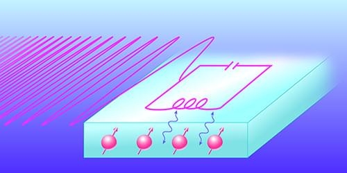
A new quantum random-access memory device reads and writes information using a chirped electromagnetic pulse and a superconducting resonator, making it significantly more hardware-efficient than previous devices.
Random-access memory (or RAM) is an integral part of a computer, acting as a short-term memory bank from which information can be quickly recalled. Applications on your phone or computer use RAM so that you can switch between tasks in the blink of an eye. Researchers working on building future quantum computers hope that such systems might one day operate with analogous quantum RAM elements, which they envision could speed up the execution of a quantum algorithm [1, 2] or increase the density of information storable in a quantum processor. Now James O’Sullivan of the London Centre for Nanotechnology and colleagues have taken an important step toward making quantum RAM a reality, demonstrating a hardware-efficient approach that uses chirped microwave pulses to store and retrieve quantum information in atomic spins [3].
Just like quantum computers, experimental demonstrations of quantum memory devices are in their early days. One leading chip-based platform for quantum computation uses circuits made from superconducting metals. In this system, the central processing is done with superconducting qubits, which send and receive information via microwave photons. At present, however, there exists no quantum memory device that can reliably store these photons for long times. Luckily, scientists have a few ideas.

Turing’s machine should sound familiar for another reason. It’s similar to the way ribosomes read genetic code on ribbons of RNA to construct proteins.
Cellular factories are a kind of natural Turing machine. What Leigh’s team is after would work the same way but go beyond biochemistry. These microscopic Turing machines, or molecular computers, would allow engineers to write code for some physical output onto a synthetic molecular ribbon. Another molecule would travel along the ribbon, read (and one day write) the code, and output some specified action, like catalyzing a chemical reaction.
Now, Leigh’s team says they’ve built the first components of a molecular computer: A coded molecular ribbon and a mobile molecular reader of the code.

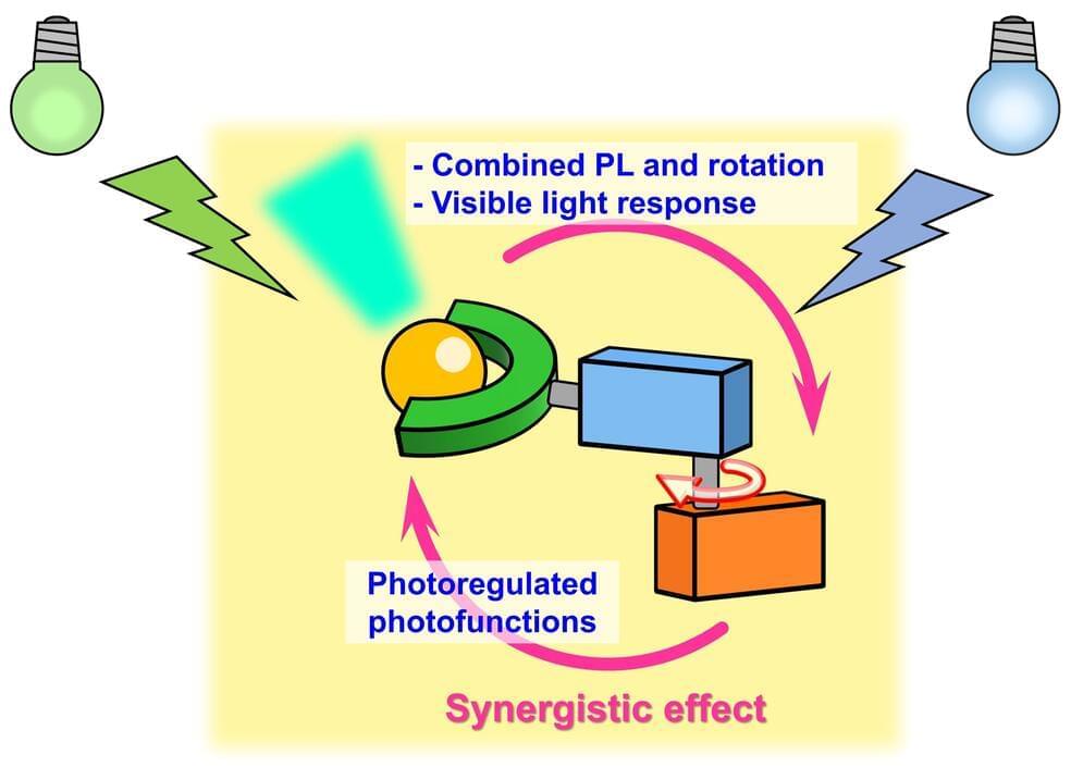
Rotary molecular motors were first created in 1999, in the laboratory of Ben Feringa, Professor of Organic Chemistry at the University of Groningen. These motors are driven by light. For many reasons, it would be good to be able to make these motor molecules visible. The best way to do this is to make them fluoresce. However, combining two light-mediated functions in a single molecule is quite challenging. The Feringa laboratory has now succeeded in doing just that, in two different ways. These two types of fluorescing light-driven rotary motors were described in Nature Communications (September 30) and Science Advances (November 4).
“After the successful design of molecular motors in the past decades, an important next goal was to control various functions and properties using such motors,” explains Feringa, who shared in the Nobel Prize in Chemistry in 2016. “As these are light-powered rotary motors, it is particularly challenging to design a system that would have another function that is controlled by light energy, in addition to the rotary motion.”
Feringa and his team were particularly interested in fluorescence since this is a prime technique that is widely used for detection, for example in biomedical imaging. Usually, two such photochemical events are incompatible in the same molecule; either the light-driven motor operates and there is no fluorescence or there is fluorescence and the motor does not operate. Feringa says, “We have now demonstrated that both functions can exist in parallel in the same molecular system, which is rather unique.”
A 3D-printed device in a tank of water braids nanowires and moves microparticles.
New antennae to access higher and higher frequency ranges will be needed for the next generation of phones and wireless devices. One way to make antennae that work at tens of gigahertz — the frequencies needed for 5G and higher devices — is to braid filaments about 1 micrometer in diameter. However, today’s industrial fabrication techniques won’t work on fibers that small.
“It was a shout-out-loud-in-joy moment when — on our first try — we crossed two fibers using only a piece of plastic, a water tank, and a stage that moves up and down.” —
Solar cells that are stretchable, flexible and wearable won the day and the best poster award from a pool of 215 at Research Expo 2016 April 14 at the University of California San Diego. The winning nanoengineering researchers aim to manufacture small, flexible devices that can power watches, LEDs and wearable sensors. The ultimate goal is to design and build much bigger flexible solar cells that could be used as power sources and shelter in natural disasters and other emergencies.
Research Expo is an annual showcase of top graduate research projects for the Jacobs School of Engineering at UC San Diego. During the poster session, graduate students are judged on the quality of their work and how well they articulate the significance of their research to society. Judges from industry, who often are alumni, pick the winners for each department. A group of faculty judges picks the overall winner from the six department winners.
This year, in addition to solar cells, judges recognized efforts to develop 3D skeletal muscle on a chip; a better way to alleviate congestion in data center networks; a nano-scale all-optical sensor; fiber optic strain sensors for structural health monitoring; and a way to predict earthquake damage in freestanding structural systems.

Traumatic brain injuries might have faded from the headlines since the NFL reached a $765 million settlement for concussion-related brain injuries, but professional football players aren’t the only ones impacted by these injuries. Each year, between 2 million and 3 million Americans suffer from traumatic brain injuries—from elderly people who fall and hit their head, to adolescents playing sports or falling out of trees, to people in motor vehicle accidents.
There are currently no treatments to stop the long-term effects of a traumatic brain injury (TBI), and accurate diagnosis requires a visit to a medical center for a CT scan or MRI, both of which involve large, expensive equipment.
UC San Diego bioengineering Professor Ester Kwon, who leads the Nanoscale Bioengineering research lab at the Jacobs School of Engineering, aims to change that. Kwon’s team is developing nanomaterials—materials with dimensions on the nanometer scale—that could be used to diagnose traumatic brain injury on the spot, be it a sports field, the scene of a car accident, or a clinical setting. They’re also engineering nanoparticles that could target the portion of the patient’s brain that was injured, delivering specific therapeutics to treat the injury and improve the patient’s long-term quality of life.

As nanotechology burrows into an increasing number of medical technologies, new developments in nanoparticles point to the ways that treatments can today be nanotechnologically targeted. In one case, would-be end effectors on microrobots are aimed at clearing up cases of bacterial pneumonia. In another, a smart-targeting system may decrease clotting risks in dangerous cases of thrombosis.
Scientists from the University of California, San Diego, demonstrated antibiotic-filled nanoparticles that hitch a ride on microbots made of algae to deliver targeted therapeutics. Their paper was recently published in Nature Materials. As a proof of concept, the researchers administered antibiotic-laden microbots to mice infected with a potentially fatal variety of pneumonia (a strain that is common in human patients who are receiving mechanical ventilation in intensive-care settings). All infections in the treated mice cleared up within a week, while untreated mice died within three days.
The algae–nanoparticle hybrid microbots were effectively distributed to infected tissue through lung fluid and showed negligible toxicity. “Our goal is to do targeted drug delivery into more challenging parts of the body, like the lungs,” said bioengineering professor Liangfang Zhang in a press statement. “And we want to do it in a way that is safe, easy, biocompatible, and long lasting.”
To produce the next generation of high-frequency antennae for 5G, 6G and other wireless devices, a team at the Harvard John A. Paulson School of Engineering and Applied Sciences (SEAS) has invented the machine and manufacturing technique to manipulate microscopic objects using 3D printing and braid them into filaments a mere micrometre in diameter.
How small is this? One human hair varies in diameter between 20 and 200 micrometres from tip to root. Spider web silk can vary from 3 to 8 micrometres in diameter. So that’s teeny tiny. And for us to pack in the many antennae that go into mobile phone technology today, the smaller the better.
Current manufacturing techniques can’t make one-micrometre filaments. But the machine invented by the Harvard SEAS team can. How does it do it? It uses the surface tension of water to grab and manipulate micromaterials. The capillary forces in the water are harnessed to help in the assembly using the variable width channels contained within the machine. Using 3D printing and the hydrophilic properties of the machine’s walls, the team used surface tension to guide kevlar nanowires attached to small floats which as they travelled through the device plaited into micrometre-scale braids.