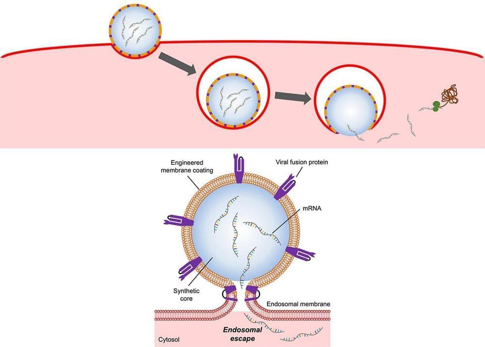
БЛОГ

Archive for the ‘nanotechnology’ category: Page 199

May 16, 2017

3D Printed multilayer circuit boards using nanomaterial inks

Posted by in categories: 3D printing, nanotechnology

Nano Dimension (NASDAQ, TASE: NNDM) is focused on the research and development of advanced 3D printed electronics, including a 3D printer for multilayer printed circuit boards, and the development of nanotechnology-based conductive and dielectric inks, which are complementary products for 3D printers.

Nextbigfuture interviewed Amit Dror, CEO and cofounder of Nano Dimension. Amit is a project leader with extensive experience in company and account management.

Nano Dimension’s novel and proprietary technologies enable the use of conductive and dielectric inks for ultra-rapid prototyping of complex, high-performance multilayer circuit boards. The company’s PCB 3D printer is the result of combining advanced breakthroughs in inkjet technology, 3D printing and nanotechnology.

Continue reading “3D Printed multilayer circuit boards using nanomaterial inks” »

May 14, 2017

Hydrogen bonds directly detected for the first time

Posted by in categories: nanotechnology, particle physics

For the first time, scientists have succeeded in studying the strength of hydrogen bonds in a single molecule using an atomic force microscope. Researchers from the University of Basel’s Swiss Nanoscience Institute network have reported the results in the journal Science Advances.

Hydrogen is the most common element in the universe and is an integral part of almost all organic compounds. Molecules and sections of macromolecules are connected to one another via , an interaction known as hydrogen bonding. These interactions play an important role in nature, because they are responsible for specific properties of proteins or nucleic acids and, for example, also ensure that water has a high boiling temperature.

To date, it has not been possible to conduct a spectroscopic or electron microscopic analysis of hydrogen and the in single molecules, and investigations using have also not yielded any clear results.

Read more

May 8, 2017

Generating power from polluted air

Posted by in categories: energy, nanotechnology, sustainability

Researchers from the University of Antwerp and KU Leuven (University of Leuven), Belgium, have developed a process that purifies air, and at the same time, generates power. The device must only be exposed to light in order to function.

“We used a small with two rooms separated by a membrane,” explained professor Sammy Verbruggen (UAntwerp/KU Leuven). “Air is purified on one side, while on the other side, is produced from a part of the degradation products. This gas can be stored and used later as fuel, as is already being done in some hydrogen buses, for example.”

In this way, the researchers respond to two major social needs: clean air and alternative energy production. The heart of the solution lies at the membrane level, where the researchers use specific nanomaterials. “These catalysts are capable of producing hydrogen gas and breaking down air pollution,” explains professor Verbruggen. “In the past, these cells were mostly used to extract hydrogen from water. We have now discovered that this is also possible, and even more efficient, with .”

Read more

May 8, 2017

Startup Promises Immortality Through AI, Nanotechnology, and Cloning

Posted by in categories: biotech/medical, life extension, nanotechnology, Ray Kurzweil, robotics/AI

They plan to record personality, memory, and body function information, and recreate it.

Read more

May 6, 2017

How Nanotech Bandages Could Supercharge First Aid

Posted by in category: nanotechnology

Scientists are developing ointments and bandages with nanoparticles that speed up and enhance healing.

Read more

May 6, 2017

Kurzweil: By 2030, Nanobots Will Flow Throughout Our Bodies

Posted by in categories: biological, nanotechnology, neuroscience, Ray Kurzweil, wearables

Another futurist, Dave Evans, founder and CTO of Silicon Valley stealth startup Stringify, gave his thoughts about Kurzweil’s nanobot idea in an interview with James Bedsole on February.

Evans explained that he thinks such a merging of technology and biology isn’t at all farfetched. In fact, he described three stages as to how this will occur: the wearable phase (where we are today), the embeddable phase (where we’re headed, with neural implants and such), and the replaceable phase.

Continue reading “Kurzweil: By 2030, Nanobots Will Flow Throughout Our Bodies” »

Apr 15, 2017

Ray Kurzweil interviews the Father of Nanotechnology Eric Drexler

Posted by in categories: computing, nanotechnology, Ray Kurzweil, solar power, sustainability

Unimaginable Radical Abundance:

Yesterday I took the time to read chapter 11 of Eric Drexler’s book Radical Abundance as to get a glimpse of what might be possible with Atomically Precise Manufacturing (APM). I highly recommend the book.

Continue reading “Ray Kurzweil interviews the Father of Nanotechnology Eric Drexler” »

Apr 14, 2017

Graphene-oxide sieve turns seawater into drinking water

Posted by in categories: nanotechnology, transportation

Schematic illustrating the direction of ion/water permeation along graphene planes (credit: J. Abraham et al./ Nature Nanotechnology)

Continue reading “Graphene-oxide sieve turns seawater into drinking water” »

Apr 12, 2017

Silver Circuits On Foil Allow Curved Touchscreens

Posted by in categories: mobile phones, nanotechnology

Microscopically fine conductor paths are required on the surfaces of smartphone touchscreens. At the edges of the appliances, these microscopic circuit paths come together to form larger connective pads. Until now, these different conductive paths had to be manufactured in several steps in time-consuming processes. With photochemical metallization, this is now possible in one single step on flexible substrates. The process has several benefits: It is fast, flexible, variable in size, inexpensive and environmentally friendly. Additional process steps for post-treatment are not necessary.

For the new process, the foils are coated with a photoactive layer of . “After that, we apply a colorless, UV-stable silver compound,” Peter William de Oliveira, head of optical materials, explains. By irradiation of this sequence of layers, the silver compound disintegrates on the photoactive layer and the silver ions are reduced to form metallic, electrically conductive silver. In this way, paths of varying sizes down to the smallest size of a thousandth of a millimeter can be achieved.

This basic principle allows conductive paths to be created individually. “There are different possibilities we can use depending on the requirements: Writing conductive paths using UV lasers is particularly suitable for the initial customized prototype manufacture and testing a new design of the conductive path. However, for mass production, this method is too time-consuming,” de Oliveira explains.

Continue reading “Silver Circuits On Foil Allow Curved Touchscreens” »

Apr 4, 2017

Nanofabrication Enables “Particle-Accelerator-on-a-Chip” Technology

Posted by in categories: biotech/medical, computing, nanotechnology

The key to this all working is the design of the nanostructures. If you just have a laser in free space, the particle will just oscillate back and forth, pushing it one way and then the other. It won’t ever gain in total energy. So you need some kind of structure that channels or modulates the fields in such a way that the particle will travel along mainly the peaks of the electromagnetic wave and not into the troughs so that it gets kicks but not deceleration.

In all of the experiments done so far, England explains that the particles are basically filling the whole wave, occupying and seeing both the peaks and troughs. This results in some particles being accelerated while others get decelerated.

“In the future, as one of the next experimental steps what we want is to bunch the particles to make very short little packets of particles that are spaced at exactly the right distance between the peaks so that they will ride only on the peaks,” says England. “So you can think of it as like… ocean waves, and you want your surfers to be positioned only on the peaks of the waves and not in the troughs.”

Continue reading “Nanofabrication Enables ‘Particle-Accelerator-on-a-Chip’ Technology” »