The development of functional nanomaterials has been a major landmark in the history of materials science. Nanoparticles with diameters ranging from 5 to 500 nm have unprecedented properties, such as high catalytic activity, compared to their bulk material counterparts. Moreover, as particles become smaller, exotic quantum phenomena become more prominent. This has enabled scientists to produce materials and devices with characteristics that had been only dreamed of, especially in the fields of electronics, catalysis, and optics.
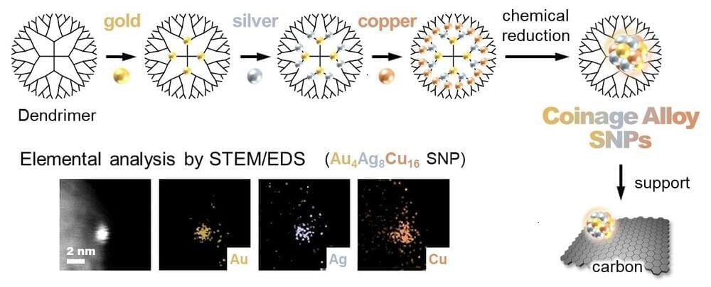
But what if we go smaller? Sub-nanoparticles (SNPs) with particle sizes of around 1 nm are now considered a new class of materials with distinct properties due to the predominance of quantum effects. The untapped potential of SNPs caught the attention of scientists from Tokyo Tech, who are currently undertaking the challenges arising in this mostly unexplored field. In a recent study published in the Journal of the American Chemical Society, a team of scientists from the Laboratory of Chemistry and Life Sciences, led by Dr. Takamasa Tsukamoto, demonstrated a novel molecular screening approach to find promising SNPs.
As one would expect, the synthesis of SNPs is plagued by technical difficulties, even more so for those containing multiple elements. Dr. Tsukamoto explains: “Even SNPs containing just two different elements have barely been investigated because producing a system of subnanometer scale requires fine control of the composition ratio and particle size with atomic precision.” However, this team of scientists had already developed a novel method by which SNPs could be made from different metal salts with extreme control over the total number of atoms and the proportion of each element.


