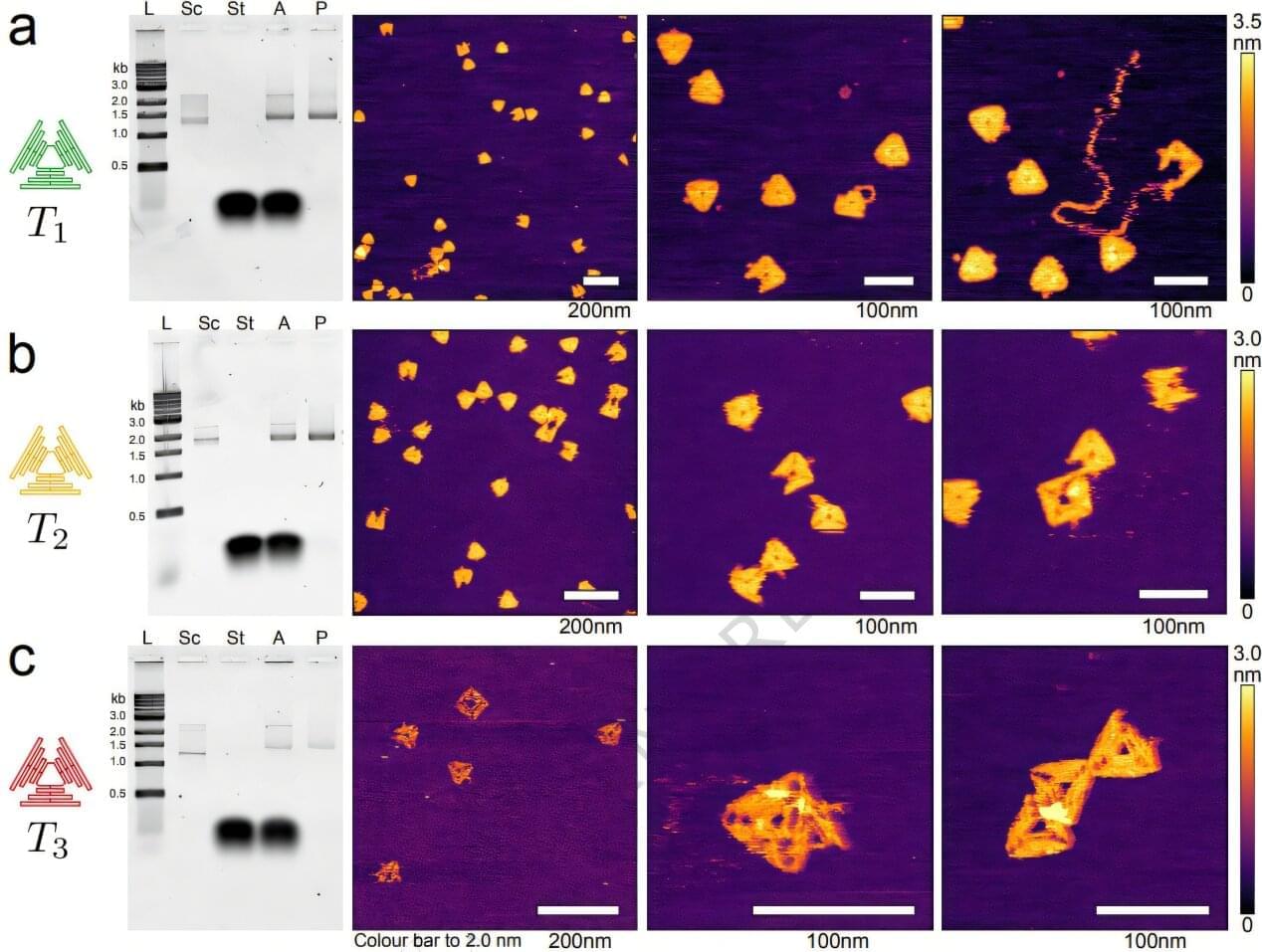
Scaffolded DNA and RNA origami is a technique that allows scientists to build tiny, highly precise two- and three-dimensional objects. Because these nanostructures can interact naturally with biological systems, they could have important future uses in health care and agritech.
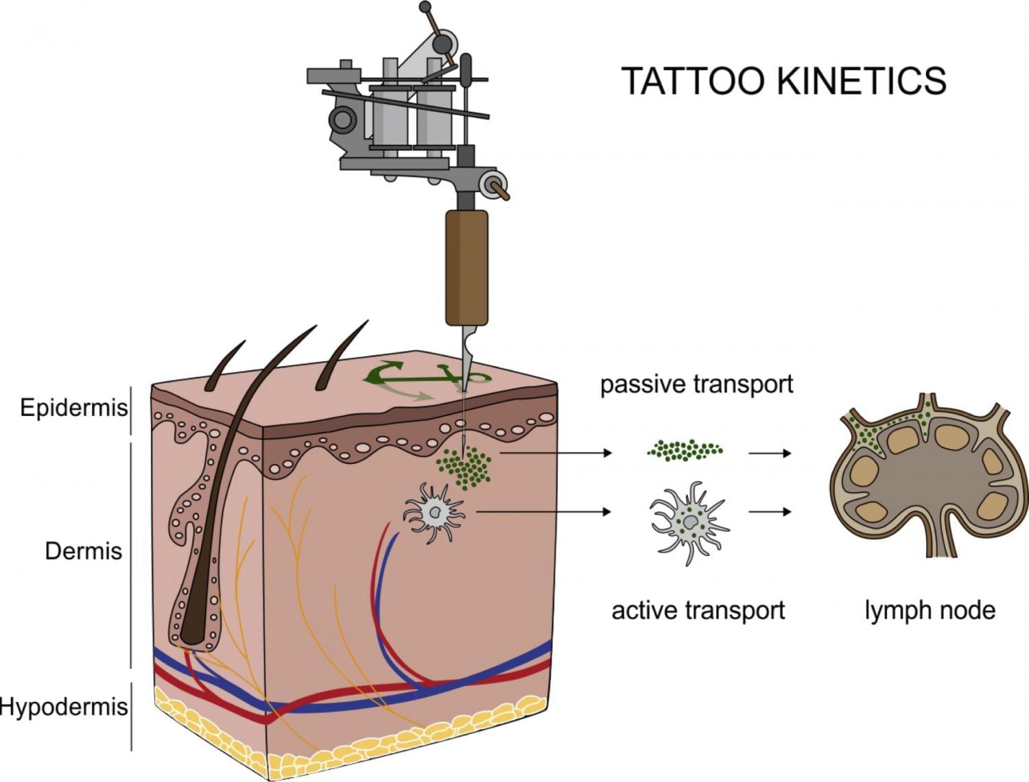
The elements that make up the ink in tattoos travel inside the body in micro and nanoparticle forms and reach the lymph nodes, according to a study published in Scientific Reports on 12 September by scientists from Germany and the ESRF, the European Synchrotron, Grenoble (France). It is the first time researchers have found analytical evidence of the transport of organic and inorganic pigments and toxic element impurities as well as in depth characterization of the pigments ex vivo in tattooed tissues. Two ESRF beamlines were crucial in this breakthrough.
“When someone wants to get a tattoo, they are often very careful in choosing a parlour where they use sterile needles that haven’t been used previously. No one checks the chemical composition of the colours, but our study shows that maybe they should,” explains Hiram Castillo, one of the authors of the study and scientist at the ESRF.
The reality is that little is known about the potential impurities in the colour mixture applied to the skin. Most tattoo inks contain organic pigments, but also include preservatives and contaminants like nickel, chromium, manganese or cobalt. Besides carbon black, the second most common ingredient used in tattoo inks is titanium dioxide (TiO2), a white pigment usually applied to create certain shades when mixed with colorants. TiO2 is also commonly used in food additives, sunscreens and paints. Delayed healing, along with skin elevation and itching, are often associated with white tattoos, and by consequence with the use of TiO2.
New research co-led by Indiana University School of Medicine scientists presents a significant step toward more precise and effective cancer treatments by using a breakthrough method to deliver therapies directly to cancer cells. The study was recently published in ACS Nano.
“One of the biggest challenges in cancer treatment is that many drugs not only attack cancer cells but also harm healthy cells throughout the body,” said Ngoc Tung Tran, Ph.D., the study’s co-lead author and an assistant professor of pediatrics and of microbiology and immunology at the IU School of Medicine. “This can lead to serious side effects and limit how well the treatment works. Our goal is to develop a smarter way to deliver cancer therapy directly to cancer cells while avoiding normal tissues.”
In the study, researchers focused on multiple myeloma, a blood cancer that mainly grows in plasma cells found in the bone marrow. Using mouse models, they carried therapeutic molecules into cells by using a delivery system of tiny, fat-based particles called lipid nanoparticles, or LNPs.
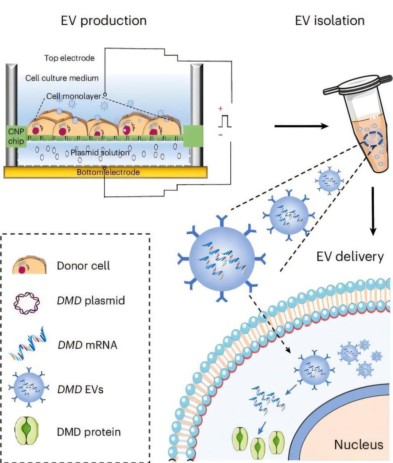
A new treatment platform developed by researchers at the University of Texas MD Anderson Cancer Center was able to deliver messenger RNA (mRNA) of the full-length DMD gene into preclinical models of Duchenne muscular dystrophy, successfully restoring the production of an important muscle protein, dystrophin, and dramatically improving muscle strength, endurance and function in vivo.
The study, published in Nature Biomedical Engineering, was co-led by Betty Kim, M.D., Ph.D., professor of neurosurgery and core member of the James P. Allison Institute, and Wen Jiang, M.D., Ph.D., associate professor of CNS Radiation Oncology.
The approach uses engineered extracellular vesicles (EVs)—natural nanoscale delivery particles—that offer distinct benefits over current viral-based gene therapies, including reduced side effects and the ability to transfer the entire DMD gene. The researchers engineered the EVs with special tags that directly target skeletal muscles after injection into the bloodstream.
Researchers boosted the sensitivity for measurements of the motion of a levitated nanoparticle, with potential uses in dark matter searches.
Researchers have a bold plan to detect unknown fundamental particles: Levitate a nanoscale object in a vacuum and watch for a microscopic recoil caused by a collision with an exotic particle. Precision measurements of macroscopic objects have been a challenge, but now a research team has demonstrated a significant sensitivity improvement with a levitated object some 6 orders of magnitude larger than in previous experiments [1]. The team hopes the method will find use in experimental searches in the next few years.
Searching for particles not accounted for by the standard model of particle physics requires experiments with unprecedented sensitivity. One method is to use laser light to levitate a small object in a vacuum, isolating it from surrounding noise. Researchers can monitor its motion and potentially detect minuscule recoils caused by rare collisions with exotic particles, such as those of dark matter.
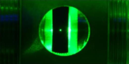
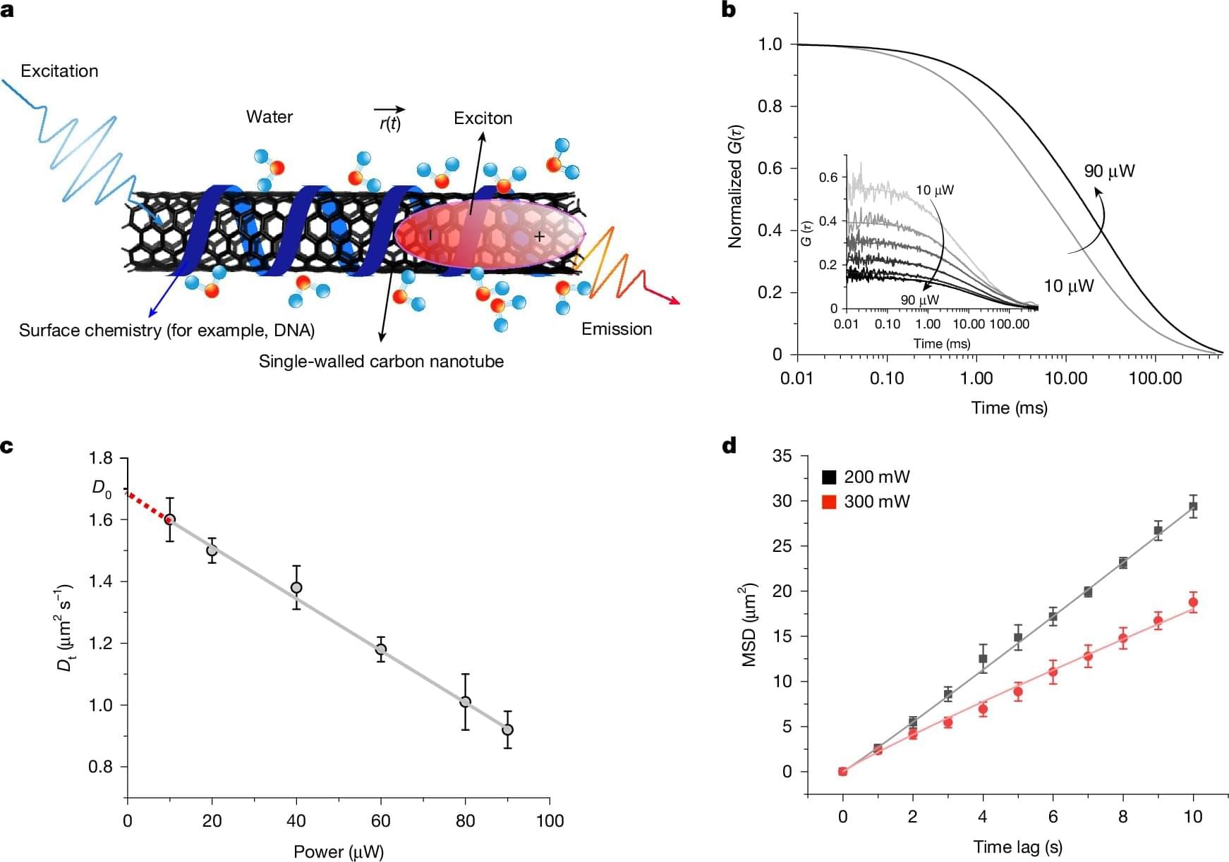
A research team in Bochum, Germany has unexpectedly found that light can slow down movements in the nanoworld. This is due to quantum friction, a phenomenon that has been poorly understood until now. The findings are published in the journal Nature.
Light is expected to heat particles up or set them in motion. However, the interdisciplinary team at Ruhr University Bochum, Germany, has now proven the opposite. In aqueous solution, fluorescent carbon nanotubes move much slower once they are irradiated with light. During this process, the diffusion constant decreases with light intensity, an effect linked to direct coupling between electrons in the solid and the molecules of the liquid.
“This discovery of light-induced quantum friction fundamentally changes our understanding of interfacial processes,” says researcher Sebastian Kruss, who led the work with Marialore Sulpizi and Martina Havenith.
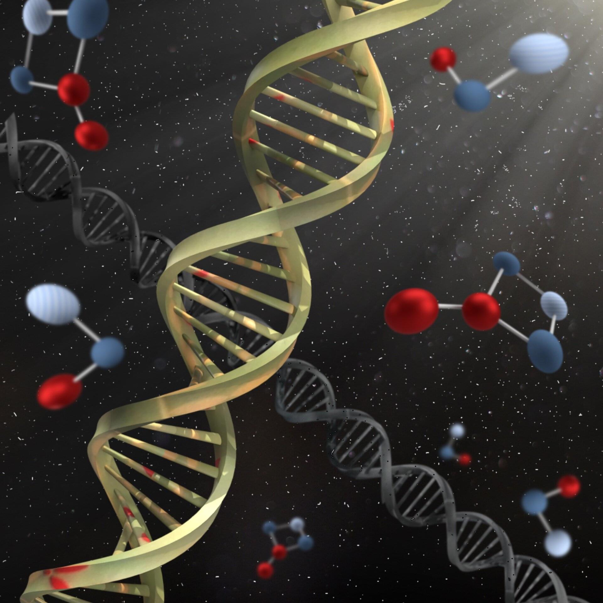
DNA is composed of long chains that act as the blueprint for living organisms. In genetic engineering, scientists cut DNA at specific sites and join the resulting fragments to other DNA sequences, enabling applications such as advanced crop breeding, treatment of genetic diseases, and the generation of animal models for drug discovery.
Assembling short DNA fragments requires overhanging sequences, known as sticky ends, to facilitate efficient binding. However, generating sticky ends requires precise cutting at targeted sites, which remains challenging with current technologies.
A Japanese research group has developed a silver nanoparticle-based technology to precisely cut and join DNA at targeted sites, achieving two to five times higher DNA assembly efficiency than conventional restriction enzyme methods. These findings were published in the journal Nucleic Acids Research.
Nanotechnology would make possible an all purpose utility belt.
This is a near-future where climate collapse is no longer theoretical, technology moves faster than ethics, and the most dangerous question is no longer can we save the planet?—but who gets to decide how?
WhiteGrass is a CliFi technothriller grounded in real science, real power structures, and deeply human consequences. It is a story about invention and control, about families forced into impossible choices, and about artificial intelligence that may be more morally awake than its creators.
Explore the characters, the science, and the ethical fault lines shaping a future that feels uncomfortably close.
According to Eliezer Yudkowsky, one of the leading thinkers in the field of AI safety and AGI alignment, the dangers associated with the development of such systems do not stop at job replacement, propaganda, and other problems related to social and economic consequences. Rather, the main threat associated with highly developed superintelligent artificial intelligence, as Yudkowsky emphasizes, is the existence of the danger that humanity would create such machines but be unable to control them properly. The author suggests the possibility that such artificial intelligence could use its biotechnological capabilities to cause disaster for the entire civilization, rapidly reach nanotechnological development milestones, and outmaneuver all attempts by humans to regulate its activities.
In the present day, as the development of artificial general intelligence progresses, there are several key questions regarding it that need to be discussed thoroughly. Thus, this fascinating interview with the noted expert covers many of these issues related to AGI and the rapid pace of research in the sphere. According to Yudkowsky, the development of ever more intelligent systems without researching how to make them safe is a serious mistake, and people should think carefully before trying this dangerous experiment again.
https://futureoflife.org ⚠️ DISCLAIMER: This channel provides AI commentary and analysis for educational and informational purposes only. Views expressed by guests are their own and do not represent the positions of any company or institution. We encourage viewers to consult multiple sources and form their own conclusions. #ai #agi #artificialintelligence.
A 90 minute interview about AI and our human future.
Dr. Hugo de Garis is a computer scientist, AI researcher, and former professor known for his early work on evolvable hardware, artificial brains, and the long-term risks of superintelligent machines. He coined and popularized the idea of the “Artilect War,” a future conflict between those who want to build godlike artificial intellects and those who believe such systems pose an existential threat to humanity. In the interview, he describes himself as trained in pure mathematics and theoretical physics, formerly a computer science professor, and now focused on broader questions about AI, cosmology, civilization, and the future of humanity.
The interview with Prof. Hugo de Garis centers on his long-standing warning that humanity may face an “Artilect War,” a civilizational conflict over whether to build godlike artificial intellects vastly superior to humans. De Garis argues that future computation, potentially extending from nanotech to femtotech and beyond, could produce minds trillions of trillions of times more capable than ours. He distinguishes between Cosmists, who want to build such beings to expand intelligence into the universe, and Terrans, who oppose them because superintelligence may eliminate or marginalize humanity. He personally remains torn, admiring the cosmic grandeur of posthuman intelligence while recognizing the existential danger.
The conversation also covers AI timelines, recursive self-improvement, AI alignment, the U.S.-China race, the Fermi paradox, simulation theory, cyborgs, cryonics, AI-generated content, the decline of universities, and the future of work. De Garis is impressed by current AI systems, treating them almost as intellectual companions, but he doubts that humanity can guarantee long-term control over recursively improving machines. The central theme is that the question “Should humanity build artilects?” may become the defining political and moral problem of the twenty-first century.