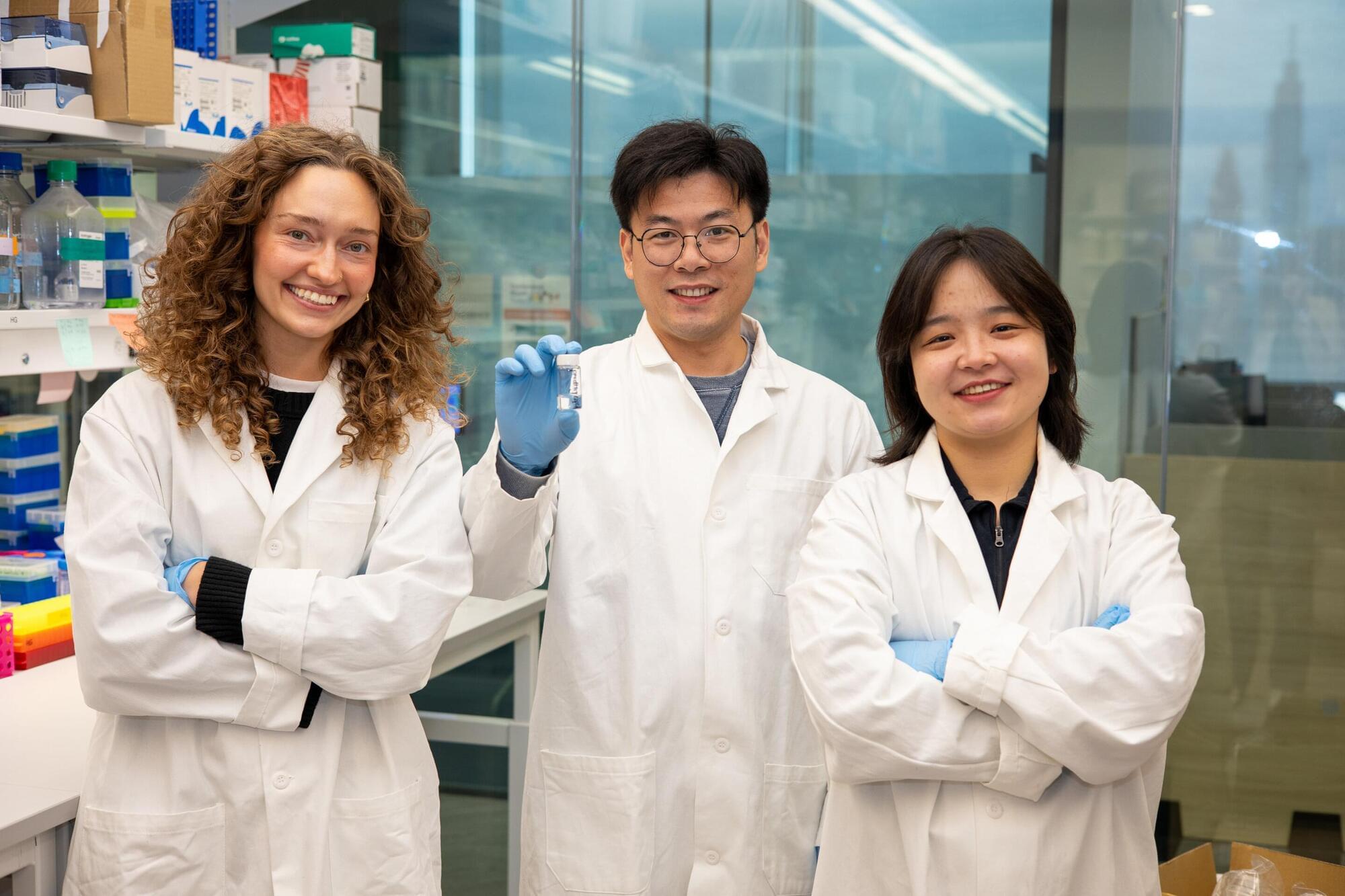
Engineers at the University of Pennsylvania have developed a new type of lipid nanoparticle (LNP) that could one day serve as a universal immunotherapy for cancers that form solid tumors, including common variants such as cancers of the breast, liver, and colon.
One of the greatest challenges in immunotherapy is the exhaustion of T cells, the white blood cells responsible for detecting and destroying cancer cells. Many tumors produce an enzyme called IDO that dampens immune activity. Over time, exposure to the harsh environment inside tumors further weakens T cells.
The new particles counter both effects at once. By delivering a drug that blocks IDO together with mRNA that instructs cells to produce an immune-activating protein, the engineered nanoparticles reinvigorate exhausted T cells, enabling them to attack tumors without the need for costly and time-consuming, patient-specific adjustments.
RIKEN researchers have demonstrated a method that can detect tiny amounts of biomarkers in liquid samples and can distinguish between highly similar biomarkers. This promises to boost the versatility and usefulness of liquid biopsies. The results are published in the Proceedings of the National Academy of Sciences.
Liquid biopsies are powerful tools for research and diagnosis since they can detect minute amounts of biomarkers in blood, saliva and urine. In particular, they are often used to detect enzymes that are connected to diseases.
“During the COVID-19 pandemic, liquid biopsies attracted unprecedented attention as a diagnostic method for infectious diseases,” notes Rikiya Watanabe of the RIKEN Molecular Physiology Laboratory. “As a result, the effectiveness of liquid biopsies is now being recognized for both testing for infectious diseases but also for a wide range of medical diagnostics.”
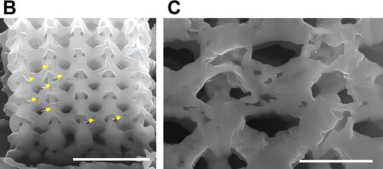
Scientists at Caltech have figured out how to precisely engineer tiny three-dimensional (3D) metallic pieces with nanoscale dimensions. The process can work with any metal or metal alloy and yields components of surprising strength despite having a porous and defect-ridden microstructure, making it potentially useful in a wide range of applications, including medical devices, computer chips, and equipment needed for space missions.
The scientists describe their method in a paper published in the journal Nature Communications. The work was completed in the lab of Julia R. Greer, the Ruben F. and Donna Mettler Professor of Materials Science, Mechanics and Medical Engineering at Caltech, and Huajian Gao of Tsinghua University in Beijing.
The researchers use a technique called two-photon lithography that allows them to sequentially build an object of a desired size and shape by carefully controlling the geometry at the level of individual voxels, the smallest distinguishable volumes, or features, in a 3D image. Beginning with a light-sensitive liquid, the scientists use a tightly focused femtosecond laser beam—a femtosecond is 1 quadrillionth of a second—to build a desired shape out of a gel-like material called hydrogel. After infusing the miniature hydrogel sculpture with metallic salts, such as copper nitrate or nickel nitrate, they heat the structure twice in a specialized furnace to produce a shrunken metallic replica of the original shape.
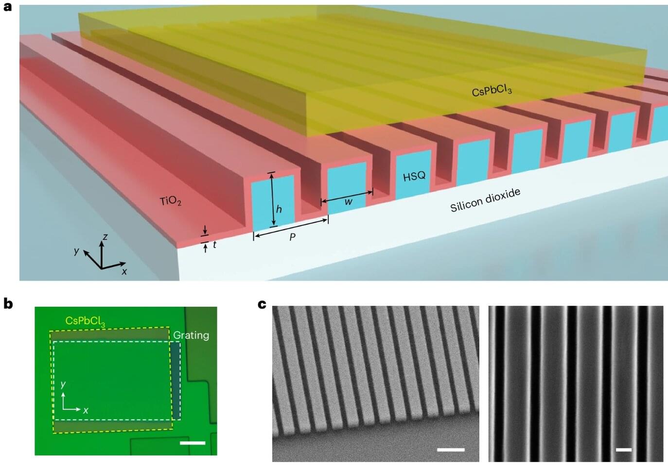
Researchers at Rensselaer Polytechnic Institute (RPI) have created a new and unusual state of matter—known as a supersolid—by engineering how light and matter interact inside a nanoscale device. The work, published in Nature Nanotechnology, demonstrates that this exotic quantum phase can exist at room temperature, overcoming a long-standing limitation in the field.
Supersolids are unusual because they combine two seemingly incompatible properties: Like a solid, they form an ordered, crystal-like structure. At the same time, they behave like a fluid, meaning they can flow without resistance. Until now, such states have only been observed under extremely cold conditions, close to absolute zero.
“Our work shows that you can create and control this exotic state using light,” said Wei Bao, Ph.D., assistant professor in the Department of Materials Science and Engineering at RPI and senior author of the study. “What’s especially exciting is that it happens at room temperature, in a platform that can be engineered and potentially scaled.”
Over the past decades, electronics engineers have been trying to develop increasingly smaller devices that can store information reliably, even when they are not powered on. A promising type of non-volatile memory device is spintronics, solid-state systems that store and process information leveraging the spin (i.e., an intrinsic form of angular momentum) of electrons.
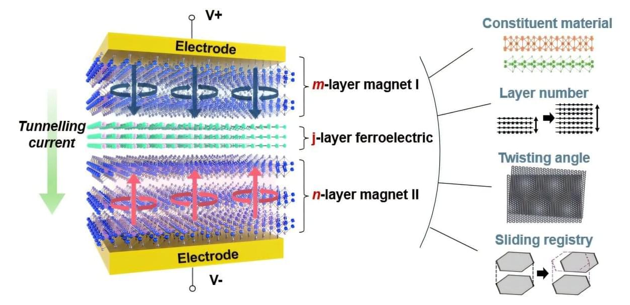
Researchers at University of Maryland and other institutes recently introduced a new spintronic device based on nanoscale structures based on materials that exhibit ferromagnetism (i.e., a permanent yet switchable magnetic order) and ferroelectricity (i.e., a permanent yet switchable electric polarization). This device, presented in a paper published in Nature Nanotechnology, can switch between four stable resistance states and could thus serve as a multistate memory.
The system that was nanoengineered by the researchers combines two different types of devices, known as magnetic tunnel junctions (MTJs) and ferroelectric tunnel junctions (FTJs). An MTJ consists of two magnetic thin films separated by an insulating thin film, while an FTJ is composed of two different metal electrode layers separated by a thin ferroelectric film. Both these types of devices have proved to be promising information storage solutions.
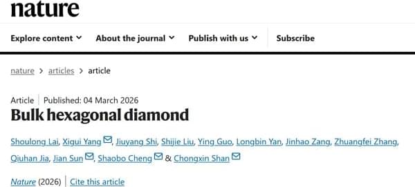
Findings of ZZU team are published online in the journal Nature. [Photo/zzu.edu.cn]
A research team from Zhengzhou University (ZZU) has successfully synthesized bulk pure-phase hexagonal diamond and precisely resolved its crystal structure, revealing a novel phase transition mechanism. The findings were published online in the journal Nature on March 5, 2026, under the title “Bulk hexagonal diamond”
Diamond, renowned for its exceptional hardness, thermal conductivity, and wide bandgap, typically adopts a cubic structure. However, the existence of a hexagonal polymorph was first predicted theoretically in 1962 and later discovered in meteorites in 1967. Yet natural samples exist only as nanoscale grains embedded in meteorites, making isolation and property measurement extremely challenging. Moreover, the high formation energy barrier of hexagonal diamond under laboratory conditions has long hindered its synthesis, fueling debate over whether it can exist as a stable bulk material.
A research team led by Lee Hyun Jun and Noh Hee Yeon from the Division of Nanotechnology at DGIST has succeeded in implementing the world’s first two-terminal-based artificial intelligence (AI) semiconductor that precisely controls hydrogen with electrical signals to enable self-learning and memory. The team’s work appears in Advanced Science.
Whereas modern AI requires the rapid processing of vast amounts of data, the separation of computation and memory in conventional computers results in speed degradation and high power consumption. “Neuromorphic semiconductors,” which perform computation and storage simultaneously by mimicking the human brain, are gaining attention as a next-generation technology that can resolve this problem. At the heart of this semiconductor is an artificial synapse device that changes its conductivity based on electrical signals and maintains that state, and the research team focused on hydrogen as the solution.
Conventional oxide-based memory devices have primarily utilized the migration of oxygen vacancies (defects) as memory. However, this has made it difficult to ensure long-term stability and uniformity between devices. In contrast, the research team solved this problem by developing its own method to precisely control the injection and discharge of hydrogen ions (H+) using an electric field.
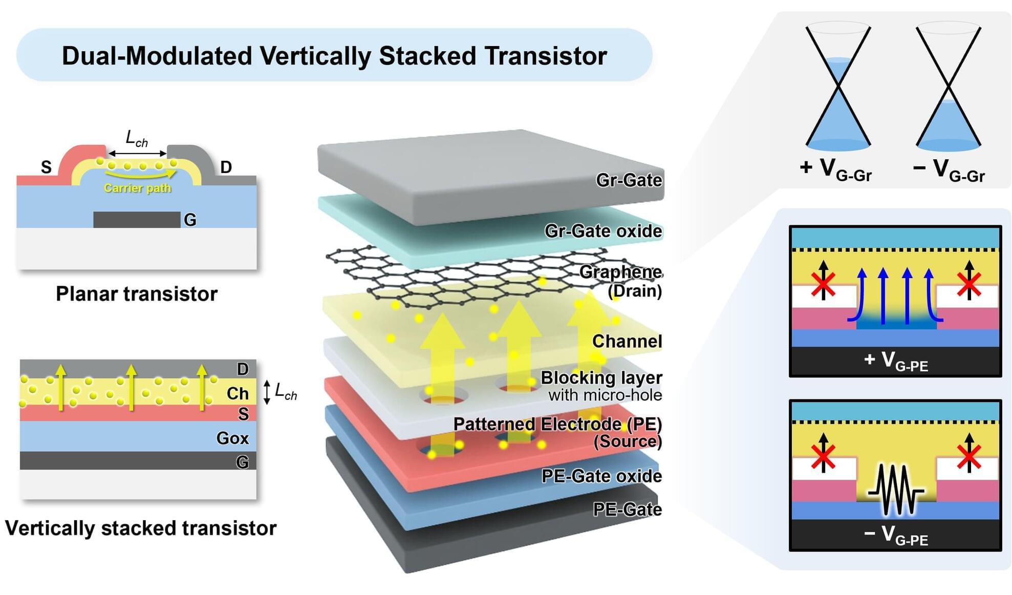
A research team led by Professor Jae Eun Jang and Dr. Goeun Pyo from the Department of Electrical Engineering and Computer Science at DGIST has developed “dual-modulated vertically stacked transistors” that operate stably without current leakage even in two-dimensional nanoscale channel structures. A study on this work is published in the journal Advanced Science.
In recent years, the semiconductor industry has faced physical limitations as the demand to integrate more devices within limited space continues to grow. To overcome these constraints, “vertically stacked transistors,” in which current-carrying channels are vertically layered, have emerged as a promising alternative for next-generation 3D semiconductors. However, conventional vertically stacked transistors suffer from a critical drawback in which gate electric signals are not delivered uniformly into the channel interior due to their electrode structure, consequently leading to current leakage or unstable device operation as the channel length becomes shorter.
To address this issue, the research team proposed a “dual-modulation structure” in which two gates—positioned above and below—control the channel through different mechanisms. This represents an innovative approach in which current flows in a sandwich-like configuration, with the upper and lower electrodes facing each other across the channel.
Could we sculpt dead planets into living worlds? From artificial crusts and orbital mirrors to taming tectonics and engineering biospheres, this is your definitive guide to turning alien rocks into second Earths.
Watch my exclusive video Fishbowl Starships — Water As Shielding — https://nebula.tv/videos/isaacarthur–… Nebula using my link for 40% off an annual subscription: https://go.nebula.tv/isaacarthur Get a Lifetime Membership to Nebula for only $300: https://go.nebula.tv/lifetime?ref=isa… Use the link https://gift.nebula.tv/isaacarthur to give a year of Nebula to a friend for just $36. Visit our Website: http://www.isaacarthur.net Support us on Patreon: / isaacarthur Support us on Subscribestar: https://www.subscribestar.com/isaac-a… Facebook Group: / 1,583,992,725,237,264 Reddit: / isaacarthur Twitter: / isaac_a_arthur on Twitter and RT our future content. SFIA Discord Server: / discord Credits: Interstellar Travel: Can We Survive The Long Journey? Episode 725; June 15, 2025 Written, Produced & Narrated by: Isaac Arthur Graphics: Jarred Eagley Jeremy Jozwik Ken York YD Visual Mafic Studios Sergio Botero Select imagery/video supplied by Getty Images Music Courtesy of Epidemic Sound http://epidemicsound.com/creator Chris Zabriskie, “Unfoldment, Revealment”, “A New Day in a New Sector”, “Oxygen Garden”, “Wonder Cycle” Kai Engel, “Endless Story About Sun and Moon” Taras Harkavyi, “Alpha and…” Dark Future, “Staring Through” pt1 Miguel Johnson. “The Commanders”, “Far From Home” Lombus, “Hydrogen Sonata”, “Cosmic Soup” Aerium, “Deijocht” Stellardrone, “Red Giant”, “Solar Eclipse”, “Billions and Billions” Chapters 0:00 Intro 5:33 What is Terraforming? 8:27 Terraforming vs Para-Terraforming 11:54 Planets vs Megastructures 14:05 Terraforming vs Bioforming 17:14 The Inevitable Hybrid Approach 20:59 Ethics & Debate: Preservation vs. Transformation 22:42 Terraforming as a Civilization-Scale Endeavor 23:46 Terraforming Technologies & Techniques 24:42 Artificial Gravity Solutions 27:58 Atmospheric Manipulation 31:25 Bioforming & Genetic Engineering 34:06 Comet & Asteroid Bombardment 39:43 Domes & Worldhouses 43:24 Geoengineering & Climate Control 47:05 Hydrospheric Engineering 49:58 Magnetosphere Generation 53:35 Fishbowl Starships 55:02 Mass & Orbital Adjustments 1:00:17 Mega-Mirrors & Solar Shades 1:04:30 Oxygenation & Soil Processing 1:07:39 Planetary Shells & Artificial Crusts 1:10:37 Terraforming Nanotechnology 1:14:04 Tidal & Seismic Stabilization 1:18:45 From Theory to Practice: Adapting Terraforming to Specific Worlds 1:20:27 Extreme Radiation Levels 1:23:57 Frequent Asteroid & Meteor Impacts 1:27:41 High Gravity 1:30:29 Highly Eccentric Orbits 1:34:46 Hostile Native Life 1:38:25 Intense Volcanism 1:40:55 Long or Erratic Day/Night Cycles 1:51:09 Low Light Levels 1:52:57 No Air 1:54:25 No Magnetosphere 1:56:17 No Seasons 1:58:13 No Water 2:00:48 Short or Long Years & Seasons 2:02:05 Tidally Locked 2:03:32 Tidally Wracked 2:04:36 Too Cold 2:05:36 Too Hot 2:06:21 Too Much Air 2:07:05 Too Much Ocean 2:08:44 Too Much Solar Wind 2:11:13 Toxic or Corrosive Atmosphere or Surface 2:14:09 Unstable Tectonics 2:15:10 Wrong Air Composition 2:16:21 Final Thoughts. Get Nebula using my link for 40% off an annual subscription: https://go.nebula.tv/isaacarthur. Get a Lifetime Membership to Nebula for only $300: https://go.nebula.tv/lifetime?ref=isa… Use the link https://gift.nebula.tv/isaacarthur to give a year of Nebula to a friend for just $36.
Visit our Website: http://www.isaacarthur.net. Support us on Patreon: / isaacarthur. Support us on Subscribestar: https://www.subscribestar.com/isaac-a… Facebook Group: / 1583992725237264 Reddit: / isaacarthur. Twitter: / isaac_a_arthur on Twitter and RT our future content. SFIA Discord Server: / discord. Credits: Interstellar Travel: Can We Survive The Long Journey? Episode 725; June 15, 2025 Written, Produced & Narrated by: Isaac Arthur. Graphics: Jarred Eagley. Jeremy Jozwik. Ken York YD Visual. Mafic Studios. Sergio Botero. Select imagery/video supplied by Getty Images. Music Courtesy of Epidemic Sound http://epidemicsound.com/creator. Chris Zabriskie, \
Nanotechnology is moving from the realm of science fiction to reality, and in the process, these tiny technologies are offering giant opportunities.
Watch my exclusive video The Fermi Paradox: Air https://nebula.tv/videos/isaacarthur–… Nebula using my link for 40% off an annual subscription: https://go.nebula.tv/isaacarthur Credits: Nanotechnology: The Future of Everything Episode 481a; January 12, 2025 Produced, Narrated & Written: Isaac Arthur Select imagery/video supplied by Getty Images Music Courtesy of Epidemic Sound http://epidemicsound.com/creator Stellardrone, “In Time”, “Red Giant” Aerium, featuring Sieger, “Deiljocht“ Get Nebula using my link for 40% off an annual subscription: https://go.nebula.tv/isaacarthur.
Credits: Nanotechnology: The Future of Everything. Episode 481a; January 12, 2025 Produced, Narrated & Written: Isaac Arthur. Select imagery/video supplied by Getty Images. Music Courtesy of Epidemic Sound http://epidemicsound.com/creator. Stellardrone, \