БЛОГ

Archive for the ‘nanotechnology’ category: Page 43

Mar 30, 2024

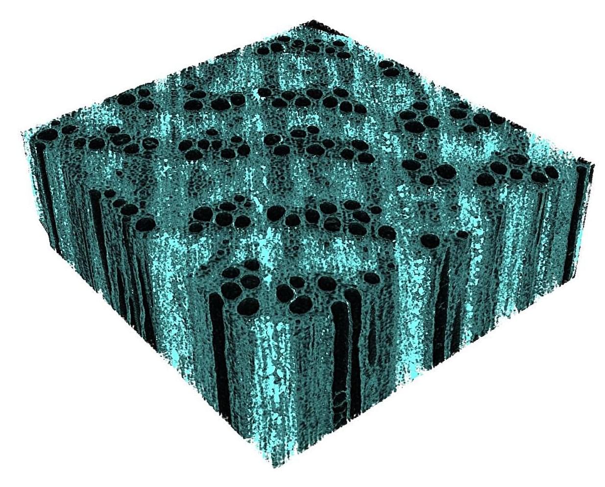
New carbon nanotube transistor enhances sensitivity and resolution of molecule glasses

Posted by in categories: biological, computing, nanotechnology

Researchers have developed a carbon nanotube (CNT) transistor for molecule glasses that facilitates detailed examination of molecular interactions. This innovative technology is poised to open a fresh research direction in nanotechnology and molecular biology.

Mar 30, 2024

A simple, scalable method using light to 3D print helical nanostructures

Posted by in categories: 3D printing, biotech/medical, nanotechnology

A new fabrication process for helical metal nanoparticles provides a simpler, cheaper way to rapidly produce a material essential for biomedical and optical devices, according to a study by University of Michigan researchers.

Mar 30, 2024

Researchers overcome lattice mismatch issue to advance optoelectronic applications

Posted by in categories: innovation, nanotechnology

A research team from City University of Hong Kong (CityU) recently successfully achieved lattice-mismatch-free construction of III-V/chalcogenide core-shell heterostructure nanowires for electronic and optoelectronic applications. This breakthrough addresses crucial technological challenges related to the lattice mismatch problem in the growth of high-quality heterostructure semiconductors, leading to enhanced carrier transport and photoelectric properties.

Mar 30, 2024

Selective operation of enhancement and depletion modes of nanoscale field-effect transistors

Posted by in categories: computing, nanotechnology

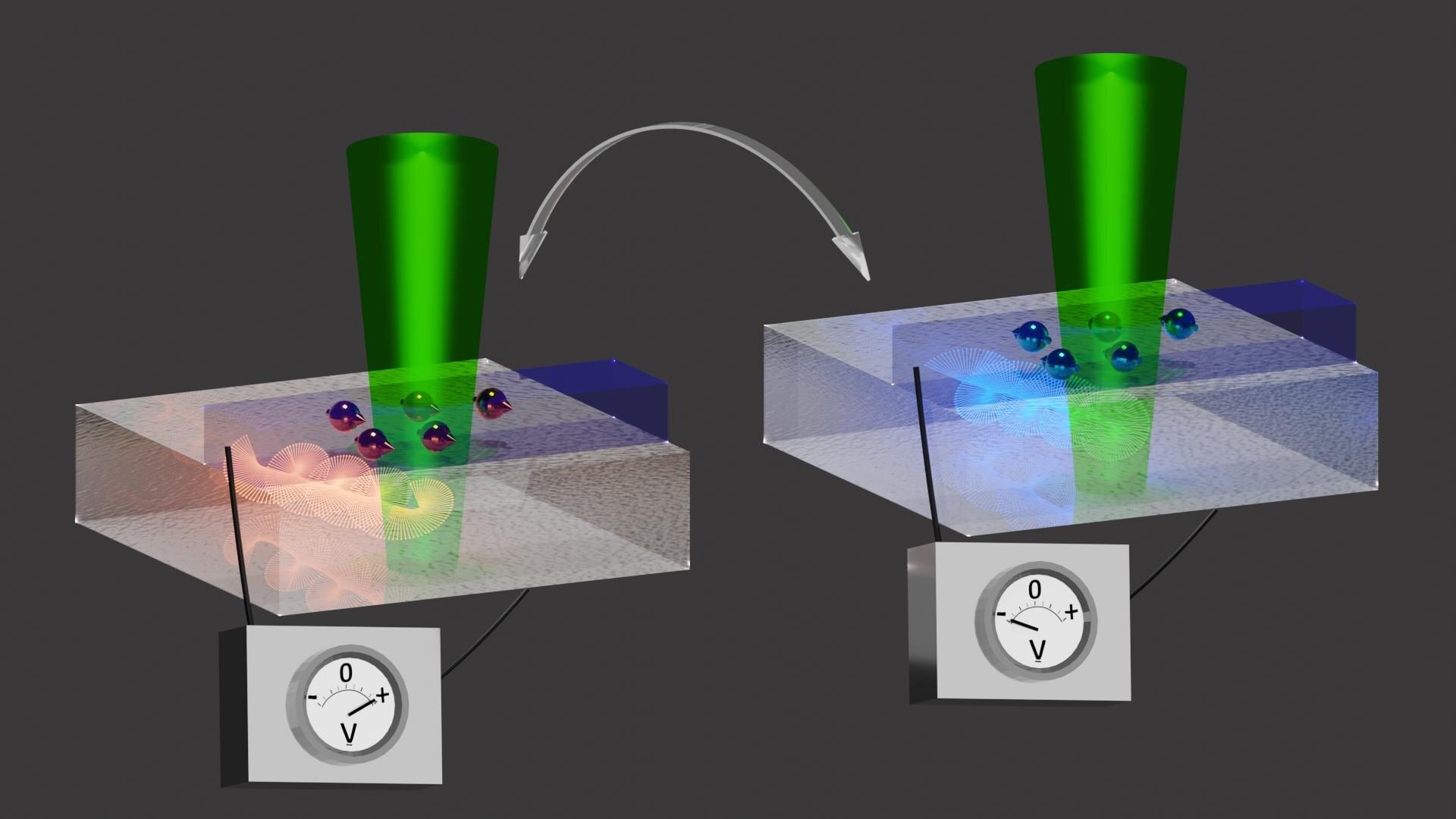
Nanoscale transistors are in demand for efficient digital circuits, and biasing of each device is critical. These stringent biasing conditions can be relaxed by obtaining precise values of the threshold voltages of the transistor. This leads to more tolerant logic states to the electrical noise.

To meet the requirements of reduced , CMOS field-effect transistors (FETs) are fabricated such that they operate in enhancement (E) mode, i.e., there are no free charge carriers in the channel at zero gate . On the other hand, depletion (D) mode transistors have higher currents than enhancement mode due to ample charge carrier density.

In contrast to switching applications of FET, for high-frequency applications, off-state of FET is not a compulsory requirement. In fact, the presence of a channel at zero gate bias is advantageous to obtain high transconductance at lower voltages. For Si FETs, the enhancement or depletion modes were determined at the fabrication step of ion implantation doping. However, it is challenging to implement this solution for the new generation of thin materials like organic semiconductors and 2D materials.

Mar 30, 2024

By Harnessing the Unlimited Vacuum Energy In Space, We Could Finally Reach Light Speed

Posted by in categories: energy, nanotechnology, space

Invisible vacuum energy is all around us. We could use it to power propulsion, enhance nanostructures, and build levitating devices.

Mar 29, 2024

Revolutionary Silicon Spikes Destroy 96% of Viruses on Contact

Posted by in categories: biotech/medical, nanotechnology

An international research team led by RMIT University has designed and manufactured a virus-killing surface that could help control disease spread in hospitals, labs, and other high-risk environments. The surface made of silicon is covered in tiny nanospikes that skewer viruses on contact.

Lab tests with the hPIV-3 virus – which causes bronchitis, pneumonia, and croup – showed 96% of the viruses were either ripped apart or damaged to the point where they could no longer replicate to cause infection. These impressive results, featured on the cover of top nanoscience journal ACS Nano, show the material’s promise for helping control the transmission of potentially dangerous biological material in laboratories and healthcare environments.

Mar 28, 2024

3D printed shapeshifting nanoparticles

Posted by in categories: materials, nanotechnology

Stanford materials engineers have 3D printed tens of thousands of hard-to-manufacture nanoparticles long predicted to yield promising new materials that change form in an instant.

Mar 28, 2024

Elusive 3D Printed Nanoparticles Could Lead to New Shapeshifting Materials

Posted by in categories: materials, nanotechnology

Stanford materials engineers have 3D printed tens of thousands of hard-to-manufacture nanoparticles long predicted to yield promising new materials that change form in an instant.

Mar 27, 2024

The mystery of fullerenes in space explained

Posted by in categories: nanotechnology, physics, space

A study from the Instituto de Astrofísica de Canarias (IAC) which combines laboratory chemistry with astrophysics, has shown for the first time that grains of dust formed by carbon and hydrogen in a highly disordered state, known as HAC, can take part in the formation of fullerenes, carbon molecules which are of key importance for the development of life in the universe, and with potential applications in nanotechnology. The results are published in the journal Astronomy & Astrophysics.

Mar 27, 2024

Construction of dual heterogeneous interface between zigzag-like Mo-MXene nanofibers and small CoNi@NC nanoparticles

Posted by in category: nanotechnology

Two-dimensional transition metal carbides (MXene) possess attractive conductivity and abundant surface functional groups, providing immense potential in the field of electromagnetic wave (EMW) absorption. However, high conductivity and spontaneous aggregation of MXene suffer from limited EMW response. Inspired by dielectric–magnetic synergy effect, the strategy of decorating MXene with magnetic elements is expected to solve this challenge.

Page 43 of 316First4041424344454647Last