Toggle light / dark theme

Two-dimensional (2D) materials, composed of a single or a few layers of atoms, are at the forefront of material science, promising revolutionary advancements in technology. These ultra-thin materials exhibit unique and exotic properties, particularly when their layers are stacked and twisted in specific ways.

This manipulation of layers can significantly alter their electronic characteristics, presenting exciting opportunities for the development of next-generation technologies such as more efficient computers and reliable electricity storage systems.

Understanding the intricate relationship between the atomic structure and electronic properties of these materials, however, poses a significant challenge. Traditional microscopy techniques struggle to capture the complete 3D atomic structure of these layered materials, especially when the layers are oriented differently or composed of light elements.

Magnetic random-access memories (MRAMs) are data storage devices that store digital data within nanomagnets, representing it in binary code (i.e., as “0” or “1”). The magnetization of nanomagnets inside these memory devices can be directed upward or downward.

Over the past decade, have introduced techniques that can switch this direction using in-plane electrical currents. These techniques ultimately enabled the creation of a new class of MRAM devices, referred to as spin-orbit torque (SOT)-MRAMs.

While existing techniques to switch magnetization direction of nanomagnets in SOT-MRAMs have proved effective, many only work if are aligned with the direction of the electric current. In a recent paper published in Nature Electronics, researchers at the National University of Singapore demonstrated the field-free switching of the perpendicular magnetic anisotropy (PMA) ferromagnet cobalt iron boron (CoFeB) at ambient conditions.

For more than 50 years, the semiconductor industry has been hard at work developing advanced technologies that have led to the amazing increases in computing power and energy efficiency that have improved our lives. A primary way the industry has achieved these remarkable performance gains has been by finding ways to decrease the size of the semiconductor devices in microchips. However, with semiconductor feature sizes now approaching only a few nanometers—just a few hundred atoms—it has become increasingly challenging to sustain continued device miniaturization.

To address the challenges associated with fabricating even smaller microchip components, the is currently transitioning to a more powerful fabrication method—extreme ultraviolet (EUV) lithography. EUV lithography employs light that is only 13.5 nanometers in wavelength to form tiny circuit patterns in a photoresist, the light-sensitive material integral to the lithography process.

The photoresist is the template for forming the nanoscale circuit patterns in the silicon semiconductor. As EUV lithography begins paving the way for the future, scientists are faced with the hurdle of identifying the most effective resist materials for this new era of nanofabrication.

When you think of empty space, you almost certainly imagine a vacuum in which nothing interesting can ever happen. However, if we zoom in to tiny length scales where quantum effects start to become important, it turns out that what you thought was empty is actually filled at all times with a seething mass of electromagnetic activity, as virtual photons flicker in and out of existence. This unexpected phenomenon is known as the vacuum fluctuation field. However, because these fluctuations of light energy are so small and fleeting in time, it is difficult to find ways for matter to interact with them, especially within a single, integrated device.

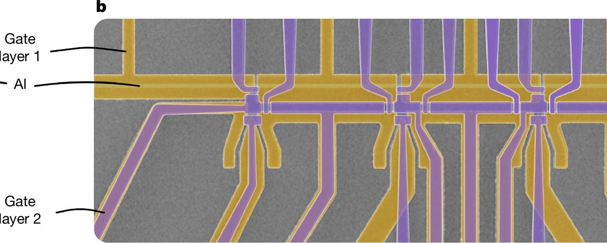
In a study published this month in Nano Letters (“Electrical Detection of Ultrastrong Coherent Interaction between Terahertz Fields and Electrons Using Quantum Point Contacts”), researchers from the Institute of Industrial Science, The University of Tokyo succeeded in fabricating a single nanoscale hybrid system for doing exactly this. In their design, a quantum point contact connects a single on-chip split-ring resonator with a two-dimensional electron system.

Quantum Hall edge channels at the quantum point contact. (Image: University of Tokyo)

In 2018, researchers reported that they had managed to get a coral larva to survive freezing and thawing for the first time. The scientists had added gold nanoparticles to their antifreeze to help the corals warm evenly during reheating. However, the thawed larvae were unable to settle and develop into adults. Instead, they kept swimming until they died.

When Narida began her experiments with hood corals in 2021, she included gold in her antifreeze recipe and combined several different antifreeze chemicals to reduce the solution’s toxicity. To thaw the animals quickly and minimize damage, Narida used a high-powered laser designed for welding jewelry. Then, she carefully washed the antifreeze away with seawater, rehydrating the corals. In the end, a whopping 11 percent of larvae in the experiment survived thawing, then settled, and developed into adults.

Leandro Godoy, a coral cryobiologist at the Federal University of Rio Grande do Sul in Brazil, is impressed by how many larvae survived after settling. “It’s a huge step,” he says, considering that, in the wild, only about five percent of corals make it that far.

HUMANS could get the power to see in the dark after mice were injected with nanoparticles which gave them the ability to see infrared light.

The rodents were given infrared night vision for 10 weeks after the injection, with only minor side effects, in an experiment conducted by Chinese and US scientists.

The team at the University of Science and Technology of China said they could modify a human’s vision to detect a wider spectrum of colours.

Hydrogen is a promising form of carbon-free energy, but moving and storing the superlight element is costly and energy-intensive. So a California startup cofounded in 2022 by two leading chemists, including a Nobel laureate, is designing a new type of tank made with nanomaterials that aims to be cheaper and safer than any currently in use — and hold more hydrogen, too.

Irvine, California-based H2MOF hopes to sell its next-generation hydrogen tanks sometime after 2024 to heavy-duty vehicle makers with plans to offer zero-emission fuel cell vehicles. It argues that in addition to holding fuel inside the vehicles, these tanks will also provide a better way to ship the fuel by truck or train as… More.


H2MOF thinks nanomaterials designed to hold hydrogen at low pressure like a sponge absorbing water are a cheaper, more efficient way to store the elemental fuel.

The research, which was published today in Nature Communications, is a joint effort by experts from the University of Sydney and the University of California at Los Angeles.

The artificial brain is made of nanowire networks, tiny wires a billion times smaller than a meter. The cables form random patterns that look like the game ‘Pick Up Sticks,’ but they also act like the neural networks in our brains. These networks can process information in different ways.