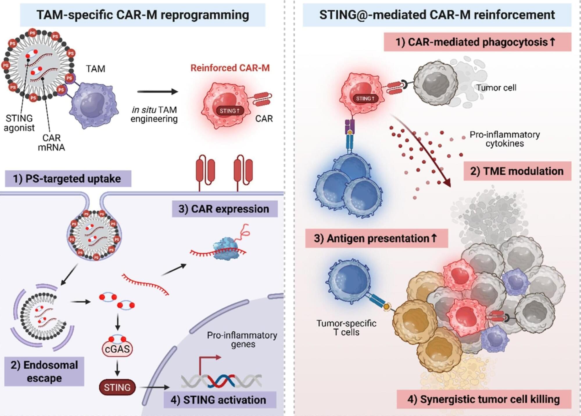
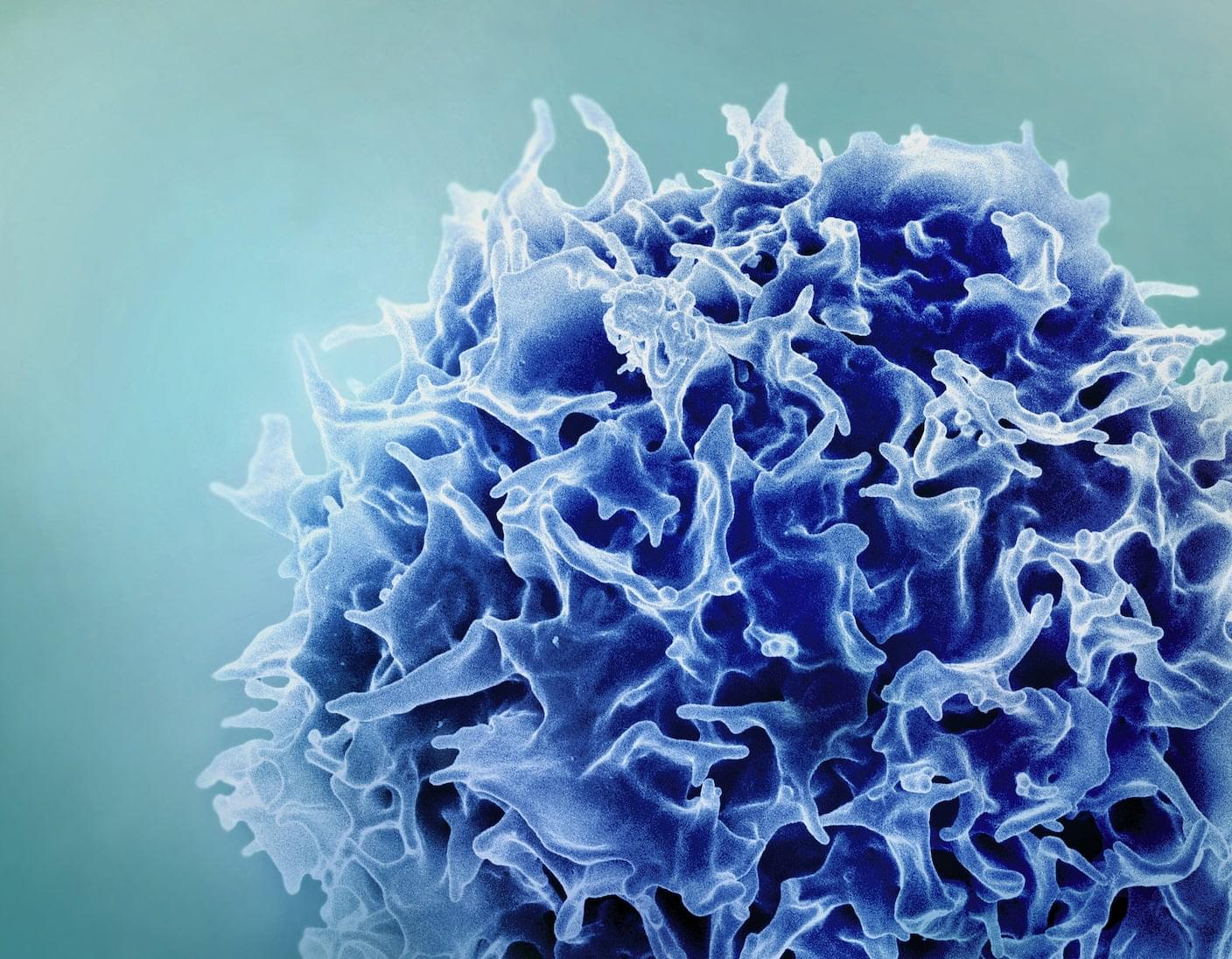
БЛОГ

Archive for the ‘nanotechnology’ category: Page 8

Nov 14, 2023

Experimental brain-like computing system more accurate with custom algorithm

Posted by in categories: biological, information science, nanotechnology, robotics/AI

An experimental computing system physically modeled after the biological brain has “learned” to identify handwritten numbers with an overall accuracy of 93.4%. The key innovation in the experiment was a new training algorithm that gave the system continuous information about its success at the task in real time while it learned. The study was published in Nature Communications.

The algorithm outperformed a conventional machine-learning approach in which training was performed after a batch of data had been processed, producing 91.4% accuracy. The researchers also showed that memory of past inputs stored in the system itself enhanced learning. In contrast, other computing approaches store memory within software or hardware separate from a device’s processor.

For 15 years, researchers at the California NanoSystems Institute at UCLA, or CNSI, have been developing a new platform technology for computation. The technology is a brain-inspired system composed of a tangled-up network of wires containing silver, laid on a bed of electrodes. The system receives input and produces output via pulses of electricity. The individual wires are so small that their diameter is measured on the nanoscale, in billionths of a meter.

Nov 13, 2023

First 2D semiconductor with 1,000 transistors developed: Redefining energy efficiency in data processing

Posted by in categories: computing, engineering, nanotechnology, transportation

As information and communication technologies (ICT) process data, they convert electricity into heat. Already today, the global ICT ecosystem’s CO2 footprint rivals that of aviation. It turns out, however, that a big part of the energy consumed by computer processors doesn’t go into performing calculations. Instead, the bulk of the energy used to process data is spent shuttling bytes between the memory to the processor.

In a paper published in the journal Nature Electronics, researchers from EPFL’s School of Engineering in the Laboratory of Nanoscale Electronics and Structures (LANES) present a new processor that tackles this inefficiency by integrating data processing and storage onto a single device, a so-called in-memory processor.

They broke new ground by creating the first in-memory processor based on a two-dimensional to comprise more than 1,000 transistors, a key milestone on the path to industrial production.

Nov 13, 2023

Online dynamical learning and sequence memory with neuromorphic nanowire networks

Posted by in categories: nanotechnology, neuroscience

Designing efficient neuromorphic systems based on nanowire networks remains a challenge. Here, Zhu et al. demonstrate brain-inspired learning and memory of spatiotemporal features using nanowire networks capable of MNIST handwritten digit classification and a novel sequence memory task performed in an online manner.

Nov 12, 2023

Using AI to optimize for rapid neural imaging

Posted by in categories: biotech/medical, nanotechnology, robotics/AI

Connectomics, the ambitious field of study that seeks to map the intricate network of animal brains, is undergoing a growth spurt. Within the span of a decade, it has journeyed from its nascent stages to a discipline that is poised to (hopefully) unlock the enigmas of cognition and the physical underpinning of neuropathologies such as in Alzheimer’s disease.

At its forefront is the use of powerful electron microscopes, which researchers from the MIT Computer Science and Artificial Intelligence Laboratory (CSAIL) and the Samuel and Lichtman Labs of Harvard University bestowed with the analytical prowess of machine learning. Unlike traditional electron microscopy, the integrated AI serves as a “brain” that learns a specimen while acquiring the images, and intelligently focuses on the relevant pixels at nanoscale resolution similar to how animals inspect their worlds.

SmartEM” assists connectomics in quickly examining and reconstructing the brain’s complex network of synapses and neurons with nanometer precision. Unlike traditional electron microscopy, its integrated AI opens new doors to understand the brain’s intricate architecture. “SmartEM: machine-learning guided electron microscopy” has been published on the pre-print server bioRxiv.

Nov 12, 2023

High-harmonic probes to unravel the secrets of spin

Posted by in categories: nanotechnology, particle physics

More sophisticated manipulation of complicated materials and their spin states at short time scales will be needed to create the next generation of spintronic devices. But, a thorough understanding of the fundamental physics underpinning nanoscale spin manipulation is necessary to fully utilize these powers for more energy-efficient nanotechnologies.

The JILA team and colleagues from institutions in Sweden, Greece, and Germany investigated the spin dynamics within a unique substance known as a Heusler compound—a combination of metals that exhibits properties similar to those of a single magnetic material. In their investigation, the scientists used a cobalt, manganese, and gallium combination that acted as an insulator for electrons with downwardly oriented spins and a conductor for those with upwardly aligned spins.

Scientists used extreme ultraviolet high-harmonic generation (EUV HHG) light as a probe to track the re-orientations of the spins inside the compound after exciting it with a femtosecond laser. Tuning the color of the EUV HHG probe light is the key to accurately interpreting the spin re-orientations.

Nov 12, 2023

Scientists use Supercomputers to make Optical Tweezers Safer for Living Cells

Posted by in categories: biotech/medical, nanotechnology, supercomputing, tractor beam

Optical tweezers manipulate tiny things like cells and nanoparticles using lasers. While they might sound like tractor beams from science fiction, the fact is their development garnered scientists a Nobel Prize in 2018.

Scientists have now used supercomputers to make optical tweezers safer to use on living cells with applications to cancer therapy, environmental monitoring, and more.

“We believe our research is one significant step closer towards the industrialization of optical tweezers in biological applications, specifically in both selective cellular surgery and targeted drug delivery,” said Pavana Kollipara, a recent graduate of The University of Texas at Austin.

Nov 11, 2023

Probing the intricate structures of 2D materials at the nanoscale

Posted by in categories: computing, nanotechnology, particle physics

Two-dimensional (2D) materials, composed of a single or a few layers of atoms, are at the forefront of material science, promising revolutionary advancements in technology. These ultra-thin materials exhibit unique and exotic properties, particularly when their layers are stacked and twisted in specific ways.

This manipulation of layers can significantly alter their electronic characteristics, presenting exciting opportunities for the development of next-generation technologies such as more efficient computers and reliable electricity storage systems.

Understanding the intricate relationship between the atomic structure and electronic properties of these materials, however, poses a significant challenge. Traditional microscopy techniques struggle to capture the complete 3D atomic structure of these layered materials, especially when the layers are oriented differently or composed of light elements.

Nov 9, 2023

Researchers demonstrate field-free switching of a commercial PMA ferromagnet at room temperature

Posted by in categories: computing, nanotechnology, open access

Magnetic random-access memories (MRAMs) are data storage devices that store digital data within nanomagnets, representing it in binary code (i.e., as “0” or “1”). The magnetization of nanomagnets inside these memory devices can be directed upward or downward.

Over the past decade, have introduced techniques that can switch this direction using in-plane electrical currents. These techniques ultimately enabled the creation of a new class of MRAM devices, referred to as spin-orbit torque (SOT)-MRAMs.

While existing techniques to switch magnetization direction of nanomagnets in SOT-MRAMs have proved effective, many only work if are aligned with the direction of the electric current. In a recent paper published in Nature Electronics, researchers at the National University of Singapore demonstrated the field-free switching of the perpendicular magnetic anisotropy (PMA) ferromagnet cobalt iron boron (CoFeB) at ambient conditions.

Nov 9, 2023

Innovative photoresist materials pave the way for smaller, high performance semiconductor chips

Posted by in categories: computing, nanotechnology, particle physics

For more than 50 years, the semiconductor industry has been hard at work developing advanced technologies that have led to the amazing increases in computing power and energy efficiency that have improved our lives. A primary way the industry has achieved these remarkable performance gains has been by finding ways to decrease the size of the semiconductor devices in microchips. However, with semiconductor feature sizes now approaching only a few nanometers—just a few hundred atoms—it has become increasingly challenging to sustain continued device miniaturization.

To address the challenges associated with fabricating even smaller microchip components, the is currently transitioning to a more powerful fabrication method—extreme ultraviolet (EUV) lithography. EUV lithography employs light that is only 13.5 nanometers in wavelength to form tiny circuit patterns in a photoresist, the light-sensitive material integral to the lithography process.

The photoresist is the template for forming the nanoscale circuit patterns in the silicon semiconductor. As EUV lithography begins paving the way for the future, scientists are faced with the hurdle of identifying the most effective resist materials for this new era of nanofabrication.

Nov 9, 2023

Communing with nothingness

Posted by in categories: computing, nanotechnology, quantum physics

When you think of empty space, you almost certainly imagine a vacuum in which nothing interesting can ever happen. However, if we zoom in to tiny length scales where quantum effects start to become important, it turns out that what you thought was empty is actually filled at all times with a seething mass of electromagnetic activity, as virtual photons flicker in and out of existence. This unexpected phenomenon is known as the vacuum fluctuation field. However, because these fluctuations of light energy are so small and fleeting in time, it is difficult to find ways for matter to interact with them, especially within a single, integrated device.

In a study published this month in Nano Letters (“Electrical Detection of Ultrastrong Coherent Interaction between Terahertz Fields and Electrons Using Quantum Point Contacts”), researchers from the Institute of Industrial Science, The University of Tokyo succeeded in fabricating a single nanoscale hybrid system for doing exactly this. In their design, a quantum point contact connects a single on-chip split-ring resonator with a two-dimensional electron system.

Quantum Hall edge channels at the quantum point contact. (Image: University of Tokyo)

Page 8 of 257First56789101112Last