БЛОГ

Archive for the ‘nanotechnology’ category: Page 98

Nov 16, 2021

Competing quantum interactions enable single molecules to stand up

Posted by in categories: computing, nanotechnology, quantum physics

Nanoscale machinery has many uses, including drug delivery, single-atom transistor technology, or memory storage. However, the machinery must be assembled at the nanoscale, which is a considerable challenge for researchers.

For nanotechnology engineers the ultimate goal is to be able to assemble functional machinery part-by-part at the nanoscale. In the macroscopic world, we can simply grab items to assemble them. It is not impossible to “grab” single anymore, but their quantum nature makes their response to manipulation unpredictable, limiting the ability to assemble molecules one by one. This prospect is now a step closer to reality, thanks to an international effort led by the Research Centre Jülich of the Helmholtz society in Germany, including researchers from the Department of Chemistry at the University of Warwick.

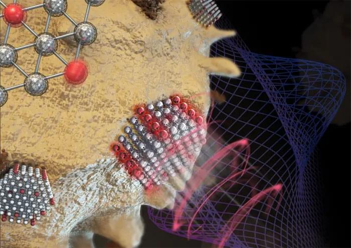
In the paper, “The stabilization potential of a standing molecule,” published today, 10 November 2021 in the journal Science Advances, an international team of researchers has been able to reveal the generic stabilization mechanism of a single standing molecule, which can be used in the rational and of three-dimensional at surfaces.

Nov 15, 2021

Construction’s Graphene Revolution Has (Finally) Begun

Posted by in categories: energy, nanotechnology

From super-strength concrete to fortified infrastructure, this is what the ‘wonder material for the 21st century’ is now bringing to construction. For more by Tomorrow’s Build subscribe now — https://bit.ly/3vOOJ98

Executive Producer and Narrator — Fred Mills.
Producer — Adam Savage.
Video Editing and Graphics — Thomas Canton.

Continue reading “Construction’s Graphene Revolution Has (Finally) Begun” »

Nov 12, 2021

“Whispering Gallery” Microresonator Can Measure Individual Nanoparticles

Posted by in categories: biotech/medical, health, nanotechnology

Forget all the nanotechnology devoted to fighting cancer, and just consider that nanoparticles have invaded makeup, anti-odor socks, sunscreen, plastic beer bottles and home pregnancy tests. Now scientists have developed a way to assess the health and environmental impact of such nanoparticles: a tiny microresonator that can detect and measure individual particles smaller than a single virus.

The microresonator is a lab-on-a-chip that harnesses the “whispering gallery” concept that’s displayed by buildings such as St. Paul’s Cathedral in London. The cathedral’s domed gallery can carry whispers easily across to the other side, but normal-volume voices end up garbled after bouncing around the dome multiple times.

Similarly, microresonators can bounce laser light many times around a circular “waveguide,” such as a glass ring. A laser frequency must perfectly fit the circumference of a ring to achieve this whispering-gallery mode.

Nov 12, 2021

Is Elon Musk’s NEURALINK ALREADY OBSOLETE? | Future of Brain Computer Interfaces

Posted by in categories: biotech/medical, Elon Musk, nanotechnology, robotics/AI, virtual reality

Elon Musk’s revolutionary company Neuralink plans to insert Computer Chips into peoples brains but what if there’s a safer and even more performant way of merging humans and machines in the future?
Enter DARPAs plan to help the emergence of non-invasive brain computer interfaces which led to the organization Battelle to create a kind of Neural Dust to interface with our brains that might be the first step to having Nanobots inside of the human body in the future.

How will Neuralink deal with that potential rival with this cutting edge technology? Its possibilities in Fulldive Virtual Reality Games, Medical Applications, merging humans with artificial intelligence and its potential to scale all around the world are enormous.

Continue reading “Is Elon Musk’s NEURALINK ALREADY OBSOLETE? | Future of Brain Computer Interfaces” »

Nov 11, 2021

Materials advancement accelerates the realization of AI technology

Posted by in categories: government, nanotechnology, robotics/AI

Researchers in Korea succeeded in developing a core material for the next-generation neuromorphic (neural network imitation) semiconductor for the first time in the country. This is a result of a research team led by Dr. Jung-dae Kwon and Yong-hun Kim of the Department of Energy and Electronic Materials of the Korea Institute of Materials Science, together with Professor Byungjin Cho’s research team at Chungbuk National University. KIMS is a government-funded research institute under the Ministry of Science and ICT.

This new concept memtransistor uses a two-dimensional nanomaterial with a thickness of several nanometers. By reproducibly imitating the electrical plasticity of nerve synapses with more than 1,000 electrical stimulations, the researchers succeeded in obtaining a high pattern recognition rate of about 94.2% (98% of simulation-based pattern recognition rate).

Molybdenum sulfur (MoS2), widely used as a , works on the principle that defects in a single crystal are moved by an external electric field, which makes it difficult to precisely control the concentration or shape of the defect. To solve the problem, the research team sequentially stacked an oxidic layer of niobium oxide (Nb2O5) and a molybdenum sulfur material and succeeded in developing an artificial synaptic device having a memtransistor structure with high electrical reliability by an external electric field. In addition, they have demonstrated that the resistance switching characteristics can be freely controlled by changing the thickness of the niobium oxidic layer, and that brain information related to memory and forgetting can be processed with a very low energy of 10 PJ (picojoule).

Nov 10, 2021

3D printing nanoresonators: Towards miniaturized and multifunctional sensors

Posted by in categories: 3D printing, mobile phones, nanotechnology

Micro-electro-mechanical devices (MEMS) are based on the integration of mechanical and electrical components on a micrometer scale. We all use them continuously in our everyday life: For example, in our mobile phones there are at least a dozen MEMS that regulate different activities ranging from motion, position, and inclination monitoring of the phone; active filters for the different transmission bands, and the microphone itself.

Even more interesting is the extreme nanoscale miniaturization of these devices (NEMS), because it offers the possibility of creating inertial, mass and with such sensitivity that they can interact with single .

However, the diffusion of NEMS sensors is still limited by the high manufacturing cost of traditional silicon-based technologies. Conversely, new technologies such as 3D printing have shown that similar structures can be created at low cost and with interesting intrinsic functionalities, but to date the performance as mass sensors are poor.

Nov 7, 2021

This New 5D Storage Technology Offers 1000 Times More Density Than Blu-Ray

Posted by in categories: biotech/medical, computing, nanotechnology

Scientists at the University of Southampton have achieved a data storage breakthrough, offering intense density and long-term archiving capabilities. With this new data storage, you can easily store up to 500 terabytes on a single CD-sized disc. Whether the data is information from museums and libraries to a person’s DNA records, it can store it all and much more!

This technology is known as five-dimensional (5D) optical storage and was first demonstrated back in 2013 when scientists were successful in using it to record and retrieve a 300-kb text file. It might not seem like much, but at that time, it was a breakthrough in data storing technologies just like how floppy discs played the same part some thousand years ago.

The data is written using a femtosecond laser which emits short but powerful pulses of light, forging tiny structures in glass that are measured in nanoscale. These structures contain information on the intensity and polarization of the laser beam in addition to the 3D space, hence it is referred as 5D data storage.

Nov 6, 2021

Semiconductor Nanowires Could Double the Efficiency of Si Solar Cells

Posted by in categories: nanotechnology, solar power, space, sustainability

Gallium arsenide (GaAs) has long been touted as the best material for making high-efficiency solar cells because of its extraordinary light absorption and electrical characteristics. It has most notably been put to use in space solar panels.

These GaAs solar cells, however, are extremely pricey to produce resulting in a demand for methods that cut down on the material usage. That’s where nanowire structures come in. These elements can potentially enhance solar cell efficiency compared to standard planar solar cells while utilizing less material.

By using GaAs in the nanowire structures, the team of researchers has found a new way to make an ultrahigh power-per-weight ratio solar cell that is more than 10 times more efficient than any other solar cell.

Nov 5, 2021

Plans Of A Technocratic Elite: ‘The Great Reset’ Is Not A Conspiracy Theory

Posted by in categories: 3D printing, biotech/medical, genetics, information science, internet, nanotechnology, quantum physics, Ray Kurzweil, robotics/AI, singularity, transhumanism

According to Klaus Schwab, the founder and executive chair of the World Economic Forum (WEF), the 4-IR follows the first, second, and third Industrial Revolutions—the mechanical, electrical, and digital, respectively. The 4-IR builds on the digital revolution, but Schwab sees the 4-IR as an exponential takeoff and convergence of existing and emerging fields, including Big Data; artificial intelligence; machine learning; quantum computing; and genetics, nanotechnology, and robotics. The consequence is the merging of the physical, digital, and biological worlds. The blurring of these categories ultimately challenges the very ontologies by which we understand ourselves and the world, including “what it means to be human.”

The specific applications that make up the 4-R are too numerous and sundry to treat in full, but they include a ubiquitous internet, the internet of things, the internet of bodies, autonomous vehicles, smart cities, 3D printing, nanotechnology, biotechnology, materials science, energy storage, and more.

While Schwab and the WEF promote a particular vision for the 4-IR, the developments he announces are not his brainchildren, and there is nothing original about his formulations. Transhumanists and Singularitarians (or prophets of the technological singularity), such as Ray Kurzweil and many others, forecasted these and more revolutionary developments,. long before Schwab heralded them. The significance of Schwab and the WEF’s take on the new technological revolution is the attempt to harness it to a particular end, presumably “a fairer, greener future.”

Nov 4, 2021

A new dimension in magnetism and superconductivity is launched

Posted by in categories: biological, chemistry, nanotechnology, particle physics

An international team of scientists from Austria and Germany has launched a new paradigm in magnetism and superconductivity, putting effects of curvature, topology, and 3D geometry into the spotlight of next-decade research. The results are published in Advanced Materials.

Traditionally, the primary field in which curvature plays a pivotal role is the theory of general relativity. In recent years, however, the impact of curvilinear geometry has entered various disciplines, ranging from solid-state physics to soft-matter physics to chemistry and biology; and giving rise to a plethora of emerging domains, such as curvilinear cell biology, semiconductors, superfluidity, optics, plasmonics and 2D van der Waals materials. In modern magnetism, superconductivity and , extending nanostructures into the has become a major research avenue because of geometry-, curvature-and topology-induced phenomena. This approach provides a means to improve conventional functionalities and to launch novel functionalities by tailoring the curvature and 3D shape.

“In recent years, there have appeared experimental and theoretical works dealing with curvilinear and three-dimensional superconducting and (anti-)ferromagnetic nano-architectures. However, these studies originate from different scientific communities, resulting in the lack of knowledge transfer between such fundamental areas of condensed matter physics as magnetism and superconductivity,” says Oleksandr Dobrovolskiy, head of the SuperSpin Lab at the University of Vienna. “In our group, we lead projects in both these topical areas and it was the aim of our perspective article to build a ‘bridge’ between the magnetism and superconductivity communities, drawing attention to the conceptual aspects of how extension of structures into the third dimension and curvilinear geometry can modify existing and aid launching novel functionalities upon solid-state systems.”