Quantum computers, systems that process information leveraging quantum mechanical effects, could outperform classical computers on some computationally demanding tasks. Despite their potential, as the size of quantum computers increases, reliably describing and measuring the states driving their functioning becomes increasingly difficult.
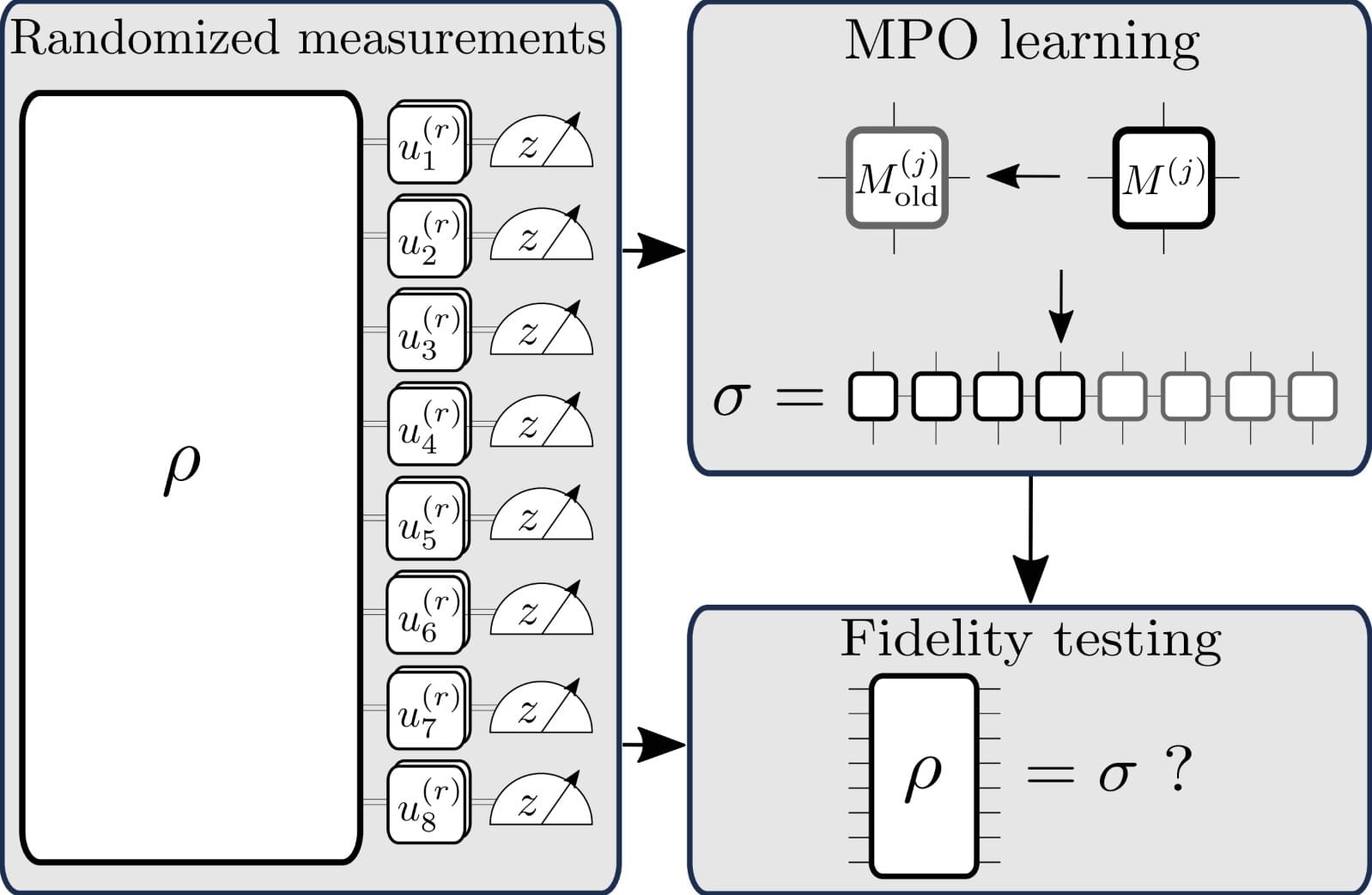
One mathematical approach to simplify the description of quantum systems entails the use of matrix-product operators (MPOs). These are mathematical representations that allow researchers to break down very large systems into a long chain of connected smaller pieces.
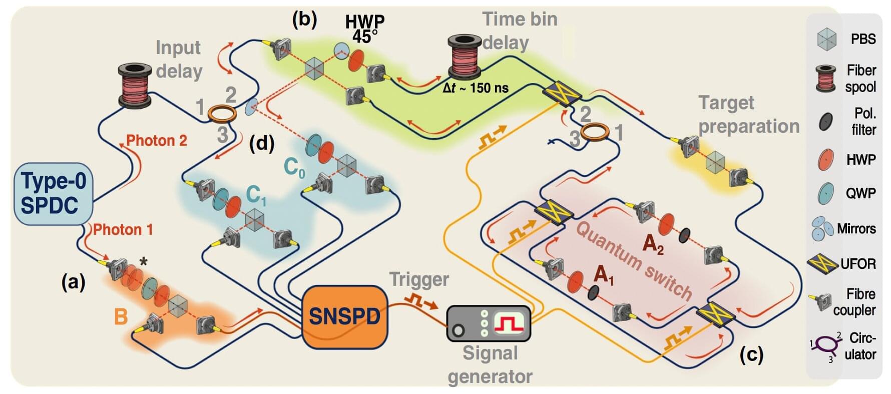
Researchers at Université Grenoble Alpes, Technical University of Munich, Max Planck Institute of Quantum Optics, University of Innsbruck and University of Bologna recently developed a new protocol that could be used to learn the MPO representations of quantum states in real, large-scale quantum experiments. Their protocol, presented in a paper published in Physical Review Letters, has so far been found to reliably reconstruct states in quantum systems including up to 96 qubits.
Civilizations at the end of time—how intelligence could survive heat death, cosmic isolation, entropy, and the universe’s longest future eras. Take back your personal data with Incogni! Use code isaacarthur at the link below and get 60% off annual plans: https://incogni.com/isaacarthur.
🛒 SFIA Merchandise: https://isaac-arthur-shop.fourthwall… Visit our Website: http://www.isaacarthur.net ❤️ Support us on Patreon: / isaacarthur ⭐ Support us on Subscribestar: https://www.subscribestar.com/isaac-a… 👥 Facebook Group: / 1,583,992,725,237,264 📣 Reddit Community: / isaacarthur 🐦 Follow on Twitter / X: / isaac_a_arthur 💬 SFIA Discord Server: / discord Credits: Civilizations at the End of Time — How Intelligence Survives the Death of the Universe Written, Produced & Narrated by: Isaac Arthur Script Editors: Andy Popescu, Briana Brownell, Connor Hogan, Darius Said, David McFarlane, Edward Nardella, Eustratius Graham, Gregory Leal, Jefferson Eagley, Keith Blockus, Konstantin Sokerin, Luca de Rosa, Ludwig Luska, Lukas Konecny, Michael Gusevsky, Mitch Armstrong, MolbOrg, Naomi Kern, Philip Baldock, Sigmund Kopperud, Steve Cardon, Tiffany Penner, Yamagishi Graphics Courtesy of: Edward Nardella, Jakub Grygier, Jarred Eagley, Jeremy Jozwik, Justin Dixon, Katie Byrne, Ken York of YD Visual, LegionTech Studios, Mafic Studios, Misho Yordanov, Murat Mamkegh, Pierre Demet, Sergio Botero, Stefan Blandin, Udo Schroeter, and Select imagery/video supplied by Getty Images Music Courtesy of: AJ Prasad, Chris Zabriskie, Dan McLeod, NeptuneUK, Lombus, Markus Junnikkala, Miguel Johnson, Phase Shift, Stellardrone, Taras Harkavyi, and Epidemic Sound: http://nebula.tv/epidemic & Stellardrone Chapters 0:00 Intro 7:11 Eternal Intelligence 49:09 Incogni 50:30 Choosing the Long Night 55:24 The Last Planet 1:27:35 When Survival Stops Being Local 1:32:38 The Omega Point 2:05:18 Big Crunch Revisited — Uncertainty Returns 2:11:09 Iron Stars 2:51:05 The Big Slurp & Vacuum Decay 2:58:23 The Big Rip 3:32:13 After the End of Time — Quantum Resurrection & Poincare Recurrence 3:34:25 Galileo. 🌐 Visit our Website: http://www.isaacarthur.net. ❤️ Support us on Patreon: / isaacarthur. ⭐ Support us on Subscribestar: https://www.subscribestar.com/isaac-a… 👥 Facebook Group: / 1583992725237264 📣 Reddit Community: / isaacarthur. 🐦 Follow on Twitter / X: / isaac_a_arthur. 💬 SFIA Discord Server: / discord. Credits: Civilizations at the End of Time — How Intelligence Survives the Death of the Universe. Written, Produced & Narrated by: Isaac Arthur. Script Editors: Andy Popescu, Briana Brownell, Connor Hogan, Darius Said, David McFarlane, Edward Nardella, Eustratius Graham, Gregory Leal, Jefferson Eagley, Keith Blockus, Konstantin Sokerin, Luca de Rosa, Ludwig Luska, Lukas Konecny, Michael Gusevsky, Mitch Armstrong, MolbOrg, Naomi Kern, Philip Baldock, Sigmund Kopperud, Steve Cardon, Tiffany Penner, Yamagishi. Graphics Courtesy of: Edward Nardella, Jakub Grygier, Jarred Eagley, Jeremy Jozwik, Justin Dixon, Katie Byrne, Ken York of YD Visual, LegionTech Studios, Mafic Studios, Misho Yordanov, Murat Mamkegh, Pierre Demet, Sergio Botero, Stefan Blandin, Udo Schroeter, and Select imagery/video supplied by Getty Images. Music Courtesy of: AJ Prasad, Chris Zabriskie, Dan McLeod, NeptuneUK, Lombus, Markus Junnikkala, Miguel Johnson, Phase Shift, Stellardrone, Taras Harkavyi, and Epidemic Sound: http://nebula.tv/epidemic & Stellardrone.
Chapters. 0:00 Intro. 7:11 Eternal Intelligence. 49:09 Incogni. 50:30 Choosing the Long Night. 55:24 The Last Planet. 1:27:35 When Survival Stops Being Local. 1:32:38 The Omega Point. 2:05:18 Big Crunch Revisited — Uncertainty Returns. 2:11:09 Iron Stars. 2:51:05 The Big Slurp & Vacuum Decay. 2:58:23 The Big Rip. 3:32:13 After the End of Time — Quantum Resurrection & Poincare Recurrence. 3:34:25 Galileo
Quantum computers, systems that process information leveraging quantum mechanical effects, could outperform classical computers on some advanced tasks. These systems rely on qubits, the fundamental units of quantum information, that become linked via an effect known as quantum entanglement and share a unified quantum state.
Qubits are known to be highly sensitive to slight changes or disturbances in their surrounding environment, also referred to as noise. Noise can prompt them to lose quantum information via a process called decoherence, which in turn leads to errors.
In recent years, quantum scientists and engineers have introduced various approaches aimed at mitigating or correcting quantum errors, with the goal of realizing fault-tolerant quantum computing. Some of these approaches rely on so-called erasure qubits, qubits whose errors are easier to detect and locate in real time.
Dark matter, a type of matter that does not emit, reflect or absorb light, is predicted to account for most of the matter in the universe. As it eludes common experimental techniques for studying ordinary matter, understanding the nature and composition of dark matter has so far proved very challenging. One hypothesis is that it is made up of hypothetical particles known as quantum chromodynamics (QCD) axions. These are theoretical elementary particles that would interact very weakly with ordinary matter and are predicted to be extremely light, highly stable and electrically neutral.
While several large-scale studies have searched for small signals or effects that would indicate the presence of these particles or their interaction with ordinary matter, their existence has not yet been confirmed experimentally. In a paper recently published in Physical Review Letters, researchers at Perimeter Institute, University of North Carolina, Kavli Institute and New York University have introduced a new approach to search for QCD axions using a class of materials that generate electric fields when deformed, called piezoelectric materials.
“The axion was proposed in the late 1970s by Weinberg and Wilczek, as a solution to the strong CP (Charge-Parity) problem, a long-standing puzzle in the theory of the strong nuclear force,” Amalia Madden, co-senior author of the paper, told Phys.org.
Can light behave like a whirlwind? It turns out it can—and such “optical tornadoes” have now been created in an extremely small structure by scientists from the Faculty of Physics at the University of Warsaw, the Military University of Technology, and the Institut Pascal CNRS at Université Clermont Auvergne. This discovery opens a new pathway for creating miniature light sources with complex structures, potentially enabling the development of simpler and more scalable photonic devices in the future, for applications such as optical communication and quantum technologies. The research is published in the journal Science Advances.
“Our solution combines several fields of physics, from quantum mechanics, through materials engineering, to optics and solid-state physics,” explains Prof. Jacek Szczytko from the Faculty of Physics at the University of Warsaw, the leader of the research group. “The inspiration came from systems known from atomic physics, where electrons can occupy different energy states. In photonics, a similar role is played by optical traps, which confine light instead of electrons.”
“You can think of it as an optical vortex,” says Dr. Marcin Muszyński from the Faculty of Physics at the University of Warsaw and Department of Physics City College of New York, the first author of the study. “The light wave twists around its axis, and its phase changes in a spiral manner. Moreover, even the polarization—the direction of oscillation of the electric field—begins to rotate.”
Researchers at the Würzburg site of the Cluster of Excellence ctd.qmat have succeeded in transferring the topological quantum Hall and spin Hall effects to a hybrid light-matter system by harnessing targeted material design. The team led by Professor Sebastian Klembt generated this optical quantum phenomenon by using polaritons—hybrid light-matter particles. This advance paves the way for optical information processing. The results have been published in Nature Communications.
Back in 1980, Nobel laureate Klaus von Klitzing, then working in Würzburg, first demonstrated topological charge transport with the quantum Hall effect.
In 2006, Professor Laurens Molenkamp at JMU Würzburg provided the world’s first experimental evidence of the quantum spin Hall effect as an intrinsic property of a topological insulator. Both phenomena protect electrons from scattering.
In a world-first, quantum physicists at ANU have observed atoms entangled in motion. Their experiment using helium atoms, represents a major advancement on similar experiments using photons, which are particles of light.
But unlike photons, helium atoms have mass and experience gravity.
Read the full article in Nature Communications: https://www.nature.com/articles/s41467-026-69070-3 development unlocks new ways to examine one of the biggest unanswered questions about the universe: how does the small-scale physics of quantum mechanics interact with gravity and general relativity at the universal scale? By observing quantum entanglement in atoms for the first time, are we one small step closer to finding out whether the “Theory of Everything” is not just hot air?
This development unlocks new ways to examine one of the biggest unanswered questions about the universe: how does the small-scale physics of quantum mechanics interact with gravity and general relativity at the universal scale?
By observing quantum entanglement in atoms for the first time, are we one small step closer to finding out whether the “Theory of Everything” is not just hot air?
Brian Greene and physicist Samir Mathur explore one of the deepest puzzles in modern physics, the true nature of black holes and the fate of information in the universe.
Their conversation centers on the black hole information paradox, a problem that has challenged physicists for decades. If quantum mechanics says information can never be destroyed, how can black holes once thought to erase everything that falls into them be reconciled with that principle? Mathur introduces the fuzzball theory, a proposal from string theory suggesting that black holes are not empty regions but complex structures that preserve information.
Greene and Mathur also revisit key developments in black hole physics, from entropy and Hawking radiation to modern ideas like firewalls and wormholes. They reflect on why certain approaches may fall short and whether recent theoretical insights are bringing the paradox closer to resolution. This conversation offers an engaging look at how physicists are rethinking black holes, quantum gravity, and the fundamental structure of reality.
This program is part of the Rethinking Reality series, supported by the John Templeton Foundation.
Participant: Samir Mathur. Moderator: Brian Greene.
For the first time, a team of physicists in Austria has carried out an experiment that appears to verify the principle of indefinite causal order: an idea that suggests that timelines of events can exist in multiple orders at the same time. Led by Carla Richter at the Vienna Center for Quantum Science and Technology, the researchers hope their result could finally allow physicists to verify a key prediction of quantum theory. The results have been published in PRX Quantum.
The basic principle of cause and effect underpins everything that happens in the classical world: for an event to occur, it must be triggered by another event in its past. Yet in the quantum world, physicists have long suspected that these rules may not always apply.
Just as quantum particles can exist in superpositions of multiple states which collapse to a single outcome when measured, indefinite causal order suggests something similar may apply to entire sequences of events. Until a measurement is made, multiple orders of cause and effect can exist in superposition.
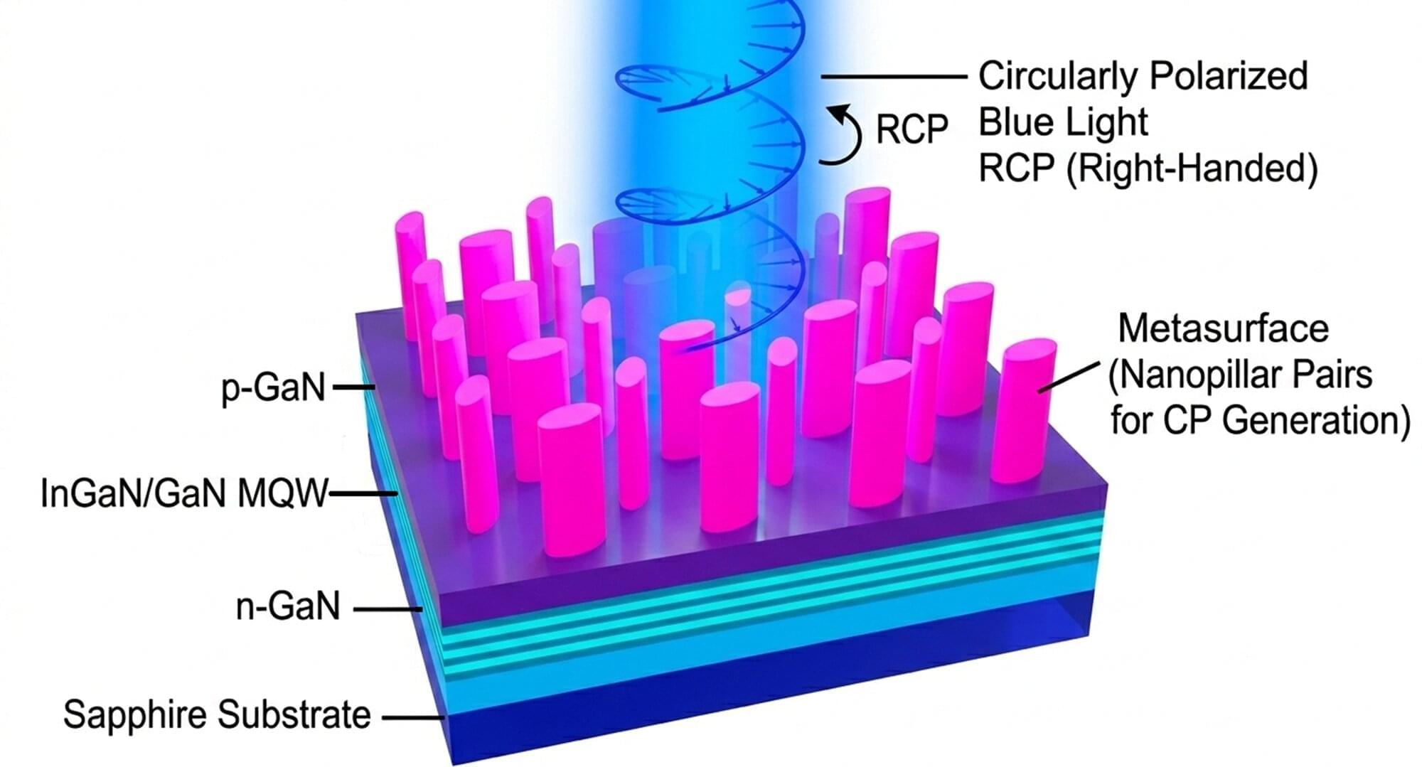
From 3D movie screens to augmented-reality devices, many modern technologies rely on our ability to manipulate light. Doing so in a cost-effective and efficient way, however, is often a formidable task. In an article published in Optics Letters, researchers from the University of Osaka announced a new light-emitting diode (LED) design that may help shrink complex optical systems into much smaller devices. The LED produces circularly polarized light using a built-in nanostructured surface, eliminating the need for bulky external optical components.
Circularly polarized light, whose electric field rotates like a corkscrew as it travels, is essential for technologies such as 3D displays, advanced imaging systems, and quantum communication tools. Traditionally, generating this kind of light requires optical components such as polarizers and special plates that modify the light’s phase. However, these components make devices larger, more complex, and harder to integrate.
“Our goal is to simplify the way circularly polarized light is produced,” says corresponding author Shuhei Ichikawa. “By integrating polarization control directly into the LED with a specially designed metasurface, we remove the need for additional optical components.”