Toggle light / dark theme

A new model suggests that lattice defects are responsible for the way some semiconductors become harder under illumination.

Understanding how semiconductors respond to illumination has been crucial to the development of photovoltaics and optical sensors. But some light-induced behaviors have been less thoroughly investigated. For example, when some semiconductors are illuminated, their mechanical properties can change drastically, a phenomenon known as photoelasticity. Photoelastic materials could be useful in the development of flexible electronics, but researchers do not understand in detail the mechanism behind the effect. Now, based on experiments and simulations, Rafael Jaramillo of the Massachusetts Institute of Technology and colleagues present a new theoretical framework that explains photoelasticity in terms of lattice defects [1].

The researchers used a diamond-tipped probe to make nanometer-scale indentations in samples of zinc oxide, zinc sulfide, and cadmium sulfide—first in the dark, and then under a range of visible and ultraviolet wavelengths. All three materials hardened to varying degrees when illuminated, with cadmium sulfide showing the largest and most consistent response. For every sample, the effect increased as the photon energy increased toward the material’s band gap.

Japanese studio Nendo has created an archive to house its products and furniture from precast concrete box culverts in central Japan.

Named Culvert Guesthouse, the archive and residence was constructed from four tunnel-like forms that were stacked on top of each other.

Designed by the studio as its own archive, the distinctive-shaped building is located in dense woodland on the edge of the town of Miyota in Nagano Prefecture.

A breakthrough from Deakin University researchers could help address a major obstacle in the development of environmentally-friendly, cost effective, polymer-based batteries.

The team from Deakin’s Institute for Frontier Materials (IFM) used modeling and simulations to design a new type of solid-state polymer electrolyte, showing its potential use in various types of polymer-based solid-state batteries, particularly sodium and potassium batteries.

Polymer-based batteries are able to support high-energy density metals in an all solid-state batteries. They use polymer as the ion conductor rather than flammable organic liquid solvents in current lithium-ion batteries. Therefore, a polymer-based solid-state battery offers an energy storage option that is greener, safer and providing a higher capacity, meaning more energy.

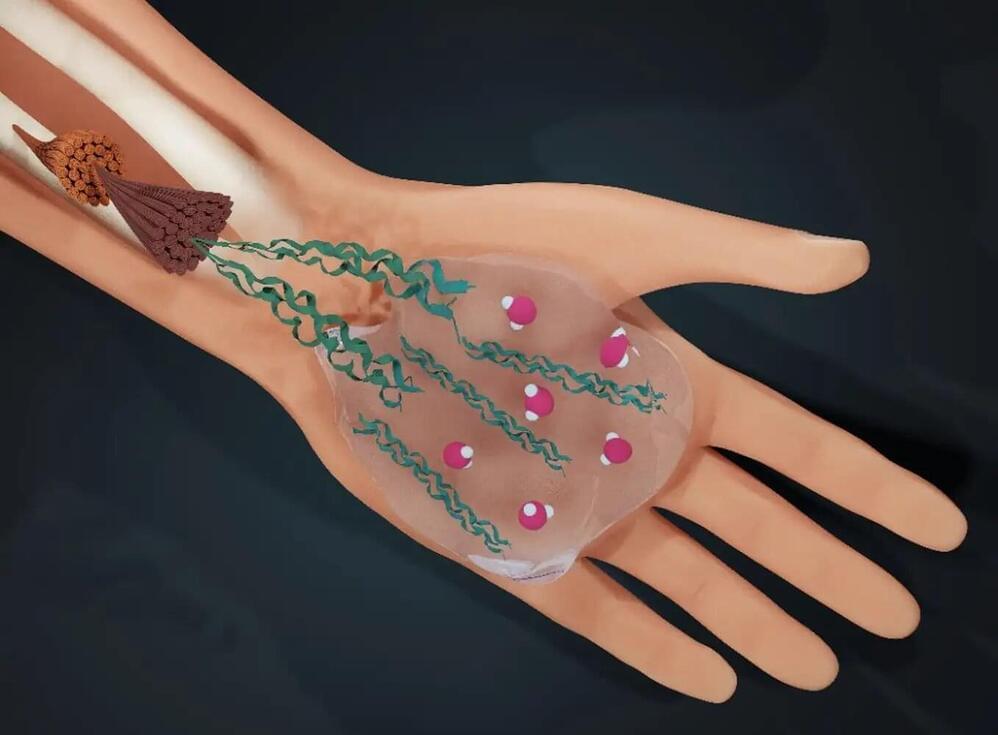
Potential applications include pressure-monitoring bandages, shade-shifting fabrics.


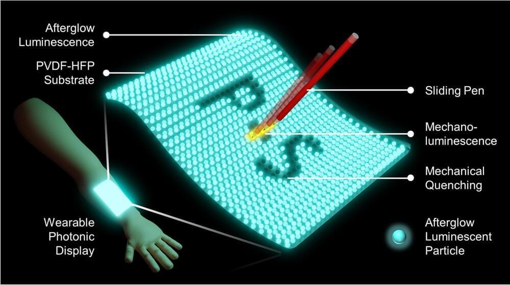
The bright iridescent colors in butterfly wings or beetle shells don’t come from any pigment molecules but from how the wings are structured—a naturally occurring example of what physicists call photonic crystals. Scientists can make their own structural colored materials in the lab, but it can be challenging to scale up the process for commercial applications without sacrificing optical precision.

Electrons find each other repulsive. Nothing personal—it’s just that their negative charges repel each other. So getting them to pair up and travel together, like they do in superconducting materials, requires a little nudge.

In old-school superconductors, which were discovered in 1911 and conduct electric current with no resistance, but only at extremely , the nudge comes from vibrations in the material’s atomic lattice.

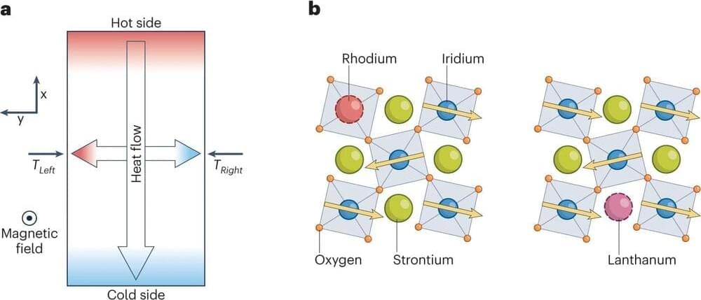
But in newer, “unconventional” superconductors—which are especially exciting because of their potential to operate at close to room temperature for things like zero-loss power transmission—no one knows for sure what the nudge is, although researchers think it might involve stripes of electric charge, waves of flip-flopping that create magnetic excitations, or some combination of things.

The CD was initially soaked in 40 mL of acetone for 1.5 minutes, releasing the metal layer by breaking down the polycarbonate substrate. The metal from the CD was easily harvested with polyimide tape, which also serves as the substrate layer in the new device integration to improve the mechanical durability and robustness of the thin metal film.

“When you pick up your hair on your clothes with sticky tape, that is essentially the same mechanism,” said Assistant Professor Ahyeon Koh, who led the research. “We loosen the layer of metals from the CD and then pick up that metal layer with tape, so we just peel it off. That thin layer is then processed and flex ible.”

Researchers created the sensors utilizing a commercially available Cricut cutter, an off-the-shelf machine for crafters that generally cut designs from materials like paper, vinyl, card stock, and iron-on transfers. The flexible circuits then would be removed and stuck onto a person. The whole fabrication process was completed in 20–30 minutes, without releasing toxic chemicals or needing expensive equipment, and it costs about $1.50 per device.