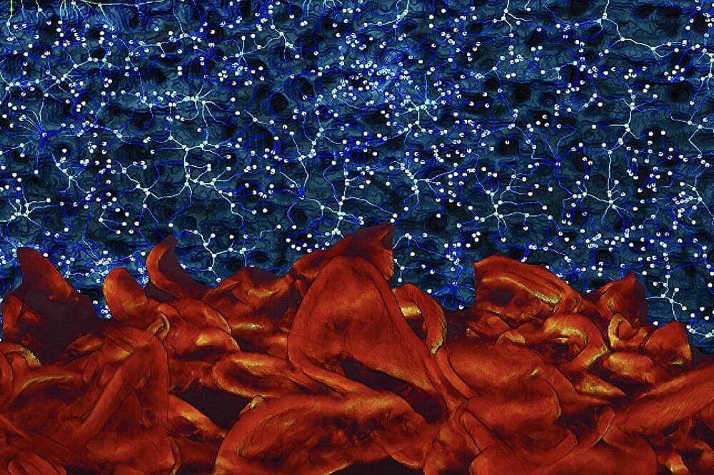
БЛОГ

Archive for the ‘nanotechnology’ category: Page 114

Mar 19, 2022

You’re invited to join our subreddit community —

Posted by in categories: bioengineering, biotech/medical, cyborgs, genetics, nanotechnology, robotics/AI, singularity, transhumanism, virtual reality

R/IntelligenceSupernova — dedicated to techno-optimists, singularitarians, transhumanist thinkers, cosmists, futurists, AI researchers, cyberneticists, crypto enthusiasts, VR creators, artists, philosophers of mind. Accelerating now towards the Cybernetic Singularity with unprecedented advances in AI & Cybernetics, VR, Biotechnology, Nanotechnology, Bionics, Genetic Engineering, Optogenetics, Neuroengineering, Robotics, and other IT fields.

Join now: https://www.reddit.com/r/IntelligenceSupernova.

#Subreddit #IntelligenceSupernova

Mar 17, 2022

Simpler graphene method paves way for new era of nanoelectronics

Posted by in categories: chemistry, nanotechnology, particle physics

Ever since its discovery in 2004, graphene has received attention owing to its extraordinary properties, among them its extremely high carrier mobility. However, the high carrier mobility has only been observed using techniques that require complex and expensive fabrication methods. Now, researchers at Chalmers report on a surprisingly high charge-carrier mobility of graphene using much cheaper and simpler methods.

“This finding shows that graphene transferred to cheap and flexible substrates can still have an uncompromisingly high mobility, and it paves the way for a new era of graphene nano-electronics,” says Munis Khan, researcher at Chalmers University of Technology.

Graphene is the one-atom-thick layer of carbon atoms, known as the world’s thinnest material. The material has become a popular choice in semiconductor, automotive and optoelectronic industry due to its excellent electrical, chemical, and material properties. One such property is its extremely .

Mar 17, 2022

Self-assembling and complex, nanoscale mesocrystals can be tuned for a variety of uses

Posted by in categories: biotech/medical, chemistry, nanotechnology, solar power

A research team from KTH Royal Institute of Technology and Max Planck Institute of Colloids and Interfaces reports to have found the key to controlled fabrication of cerium oxide mesocrystals. The research is a step forward in tuning nanomaterials that can serve a wide range of uses—including solar cells, fuel catalysts and even medicine.

Mesocrystals are nanoparticles with identical size, shape and crystallographic orientation, and they can be used as to create artificial nanostructures with customized optical, magnetic or electronic properties. In nature, these three-dimensional structures are found in coral, sea urchins and calcite desert rose, for example. Artificially-produced cerium oxide (CeO2) mesocrystals—or nanoceria—are well-known as catalysts, with antioxidant properties that could be useful in pharmaceutical development.

“To be able to fabricate CeO2 mesocrystals in a controlled way, one needs to understand the formation mechanism of these materials,” says Inna Soroka, a researcher in applied at KTH. She says the team used radiation chemistry to reveal for the first time the ceria mesocrystal formation mechanism.

Mar 17, 2022

Wax-coated sand keeps soil wet longer, improves crop yields in arid regions

Posted by in categories: biotech/medical, nanotechnology

Dry, hot regions are difficult places to grow plants because the soil dries out quickly. As a result, farmers in arid and semi-arid regions irrigate their fields with buried networks of irrigation tubing and cover the ground with plastic sheets. But plastic sheets are expensive and create waste. Now, researchers reporting in ACS Agricultural Science & Technology have developed a simple, biodegradable ground cover—wax-coated sand—which keeps soil wet and increases crop yields.

To irrigate crops, farmers usually get water from nearby waterways or underground aquifers. These supplies can be rapidly depleted when growing plants in , where the soil is comprised mostly of sand and can’t hold onto water well. One way to improve irrigated water’s efficiency is to make sure it stays in the soil long enough so that plants’ roots can take it up. Previous studies have shown that ground cover barriers, such as plastic sheets and engineered nanomaterials, can slow evaporation and enhance and . However, both could leach unwanted compounds into the soil with unknown long-term impacts. Some plants and animals naturally produce waxy substances that trap and pool water from fog or condensation so that they can access these moisture sources. Taking inspiration from nature, Himanshu Mishra and colleagues wanted to see if they could coat sand with wax, creating an environmentally benign ground cover to control soil evaporation.

The researchers chose purified paraffin wax, a biodegradable substance available in large quantities, for their experiments. They dissolved the wax in hexane and poured silica sand into the mixture. As the solvent evaporated, a 20-nm-thick coating of wax was left behind on the grains. When the team applied the wax-coated sand in a on an open field in Saudi Arabia, it decreased the loss of soil moisture up to 50–80%. Field trials revealed that tomato, barley and wheat plants mulched with the new material produced substantially more fruit and grain than those grown in uncovered soil. In addition, the microbial community around the plants’ roots and in the soil wasn’t negatively impacted by the waxy mulch, which could have acted as a food source for some of the microbes. This simple nature-inspired technology could make more efficient in arid regions, the researchers say.

Mar 14, 2022

Creating sub-1-nm gate lengths for MoS2 transistors

Posted by in categories: computing, nanotechnology, particle physics

A team of researchers working at Tsinghua University in China has created a sub-1-nm gate in a MoS2 transistor. In their paper published in the journal Nature, the group outlines how they created the super tiny gate and explains why they believe it will be difficult for anyone to beat their record.

For most of the history of microcomputing, Moore’s Law has held up—researchers and engineers have managed to double the speed and capability of computers regularly by reducing the size of their components. But more recently, it has grown increasingly difficult to make components smaller as scientists now run into . In this new effort, the researchers believe they may have bumped up against the ultimate limit—they have built a gate that is just one atom in length.

At their most basic, transistors are a source and a drain, with a gate controlling the flow of electricity between them. It switches on and off depending on how much electricity is applied. The push to reduce the size of the components has led to the testing of materials such as carbon nanotubes, which are approximately 1nm, for use as gates. In this new effort, the researchers have unrolled the and used its graphene edge as the gate—reducing its length to just 0.34 nm.

Mar 14, 2022

Scientists fabricate novel electrical component to improve stability of solar cells

Posted by in categories: internet, nanotechnology, solar power, sustainability

In the future, decarbonized societies that use internet of things (IoT) devices will become commonplace. But to achieve this, we need to first realize highly efficient and stable sources of renewable energy. Solar cells are considered a promising option, but their electrical contacts suffer from a “tradeoff” relationship between surface passivation and conductivity. Recently, researchers from Japan have developed a new type of electrical contact that can overcome this problem.

The most recent type of commercial photovoltaic cell (solar cell) uses stacked layers of crystalline silicon (c-Si) and an ultrathin layer of silicon oxide (SiOx) to form an electrical contact. The SiOx is used as a “passivating” film—an unreactive layer that improves the performance, reliability, and stability of the device. But that does not mean that simply increasing the thickness of this passivating layer will lead to improved . SiOx is an electrical insulator and there is a trade-off relationship between passivation and the conductivity of the electrical contact in solar cells.

In a new study, published in ACS Applied Nano Materials, a research team led by Assistant Professor Kazuhiro Gotoh and Professor Noritaka Usami from Nagoya University has developed a novel SiOx layer that simultaneously allows high passivation and improved conductivity. Named NAnocrystalling Transport path in Ultrathin dielectrics for REinforcing passivating contact (NATURE contact), the new electrical contact consists of three-layer structures made up of a layer of silicon nanoparticles sandwiched between two layers of oxygen-rich SiOx. “You can think of a passivating film as a big wall with gates in it. In the NATURE contact, the big wall is the SiOx layer and the gates are Si nanocrystals,” explains Dr. Gotoh.

Mar 13, 2022

The next generation of robots will be shape-shifters

Posted by in categories: nanotechnology, physics, robotics/AI

Physicists have discovered a new way to coat soft robots in materials that allow them to move and function in a more purposeful way. The research, led by the UK’s University of Bath, is described today in Science Advances.

Authors of the study believe their breakthrough modeling on ‘active matter’ could mark a turning point in the design of robots. With further development of the concept, it may be possible to determine the shape, movement and behavior of a soft solid not by its natural elasticity but by human-controlled activity on its .

The surface of an ordinary soft material always shrinks into a sphere. Think of the way water beads into droplets: the beading occurs because the surface of liquids and other soft material naturally contracts into the smallest surface area possible—i.e. a sphere. But active matter can be designed to work against this tendency. An example of this in action would be a rubber ball that’s wrapped in a layer of nano-robots, where the robots are programmed to work in unison to distort the ball into a new, pre-determined shape (say, a star).

Mar 12, 2022

New tool allows unprecedented modeling of magnetic nanoparticles

Posted by in categories: biotech/medical, chemistry, computing, nanotechnology

Researchers at North Carolina State University have developed a new computational tool that allows users to conduct simulations of multi-functional magnetic nanoparticles in unprecedented detail. The advance paves the way for new work aimed at developing magnetic nanoparticles for use in applications from drug delivery to sensor technologies.

“Self-assembling , or MNPs, have a lot of desirable properties,” says Yaroslava Yingling, corresponding author of a paper on the work and a Distinguished Professor of Materials Science and Engineering at NC State. “But it has been challenging to study them, because computational models have struggled to account for all of the forces that can influence these materials. MNPs are subject to a complicated interplay between external magnetic fields and van der Waals, electrostatic, dipolar, steric, and .”

Many applications of MNPs require an understanding of how the nanoparticles will behave in complex environments, such as using MNPs to deliver a specific protein or drug molecule to a targeted cancer affected cell using external magnetic fields. In these cases, it is important to be able to accurately model how MNPs will respond to different chemical environments. Previous computational modeling techniques that looked at MNPs were unable to account for all of the chemical interactions MNPs experience in a given colloidal or biological environment, instead focusing primarily on physical interactions.

Mar 12, 2022

A bio-inspired mechano-photonic artificial synapse

Posted by in categories: biological, nanotechnology, robotics/AI

Multifunctional and diverse artificial neural systems can incorporate multimodal plasticity, memory and supervised learning functions to assist neuromorphic computation. In a new report, Jinran Yu and a research team in nanoenergy, nanoscience and materials science in China and the US., presented a bioinspired mechano-photonic artificial synapse with synergistic mechanical and optical plasticity. The team used an optoelectronic transistor made of graphene/molybdenum disulphide (MoS2) heterostructure and an integrated triboelectric nanogenerator to compose the artificial synapse. They controlled the charge transfer/exchange in the heterostructure with triboelectric potential and modulated the optoelectronic synapse behaviors readily, including postsynaptic photocurrents, photosensitivity and photoconductivity. The mechano-photonic artificial synapse is a promising implementation to mimic the complex biological nervous system and promote the development of interactive artificial intelligence. The work is now published on Science Advances.

Brain-inspired neural networks.

The human brain can integrate cognition, learning and memory tasks via auditory, visual, olfactory and somatosensory interactions. This process is difficult to be mimicked using conventional von Neumann architectures that require additional sophisticated functions. Brain-inspired neural networks are made of various synaptic devices to transmit information and process using the synaptic weight. Emerging photonic synapse combine the optical and electric neuromorphic modulation and computation to offer a favorable option with high bandwidth, fast speed and low cross-talk to significantly reduce power consumption. Biomechanical motions including touch, eye blinking and arm waving are other ubiquitous triggers or interactive signals to operate electronics during artificial synapse plasticization. In this work, Yu et al. presented a mechano-photonic artificial synapse with synergistic mechanical and optical plasticity.

Mar 12, 2022

Synthetic synapses get more like a real brain

Posted by in categories: biological, chemistry, food, nanotechnology, robotics/AI, supercomputing

The human brain, fed on just the calorie input of a modest diet, easily outperforms state-of-the-art supercomputers powered by full-scale station energy inputs. The difference stems from the multiple states of brain processes versus the two binary states of digital processors, as well as the ability to store information without power consumption—non-volatile memory. These inefficiencies in today’s conventional computers have prompted great interest in developing synthetic synapses for use in computers that can mimic the way the brain works. Now, researchers at King’s College London, UK, report in ACS Nano Letters an array of nanorod devices that mimic the brain more closely than ever before. The devices may find applications in artificial neural networks.

Efforts to emulate biological synapses have revolved around types of memristors with different resistance states that act like memory. However, unlike the the devices reported so far have all needed a reverse polarity to reset them to the initial state. “In the brain a change in the changes the output,” explains Anatoly Zayats, a professor at King’s College London who led the team behind the recent results. The King’s College London researchers have now been able to demonstrate this brain-like behavior in their synaptic synapses as well.

Zayats and team build an array of gold nanorods topped with a polymer junction (poly-L-histidine, PLH) to a metal contact. Either light or an electrical voltage can excite plasmons—collective oscillations of electrons. The plasmons release hot electrons into the PLH, gradually changing the chemistry of the polymer, and hence changing it to have different levels of conductivity or light emissivity. How the polymer changes depends on whether oxygen or hydrogen surrounds it. A chemically inert nitrogen chemical environment will preserve the state without any energy input required so that it acts as non-volatile memory.