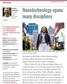
БЛОГ

Archive for the ‘nanotechnology’ category: Page 207

Jan 19, 2017

Engineers Australia : New lab-made diamond at mining’s cutting-edge

Posted by in categories: materials, nanotechnology

Australia getting their QC production lines ready with this advancement. BTW — get ready as the printers are coming soon.


The Australian National University (ANU) has led an international team to create a nano-sized diamond that’s harder than the natural gem and which will be useful for cutting through super-hard mining materials.

ANU Associate Professor Jodie Bradby said her team, including ANU PhD student Thomas Shiell and experts from RMIT, the University of Sydney and the United States, fabricated nano-sized Lonsdaleite, which is a hexagonal diamond only found in nature at meteorite impact sites, such as in Arizona’s Canyon Diablo.

Continue reading “Engineers Australia : New lab-made diamond at mining’s cutting-edge” »

Jan 19, 2017

Computers Made of Genetic Material Will Revolutionize Our World

Posted by in categories: biotech/medical, computing, genetics, nanotechnology

Researchers have been able to create tiny structures for conducting electricity by using DNA and gold plating. This new nanostructure could be the foundation of future electronics as soon as improvements are made on this breakthrough development.

Read more

Jan 18, 2017

Memristor can do multistate processing as well as nonvolatile memory

Posted by in categories: computing, nanotechnology, neuroscience, quantum physics

Nice; ReRam with multi-state processing and reliable storage.


Short of full blown molecular computers or universal quantum computers or optical computers memristors have the most potential for a hardware change to dramatically boost the power and capabilities of computers. The boost to computer power could be nearly a million times by fully leveraging memristors. It would likely be more like a thousand times with more near to mid term usage of memristors.

Memristors (aka ReRAM) could become computer memory that is over 10 times denser than Flash or DRAM in two dimensions. Memristors like flash would be nonvolatile memory that would not need power for retain memory. Memristors are created from nanowire lattices which could be stacked in three dimensions. Memristors have also previously been shown to behave like brain synapses which could be used for computer architectures that emulate the human brain for neuromorphic computing. Now there is work on multistate memristors that perform computation. This means that eventually processing and memory could be tightly integrated.

Continue reading “Memristor can do multistate processing as well as nonvolatile memory” »

Jan 18, 2017

Explaining how 2-D materials break at the atomic level

Posted by in categories: nanotechnology, physics

Cracks sank the ‘unsinkable’ Titanic; decrease the performance of touchscreens and erode teeth. We are familiar with cracks in big or small three-dimensional (3D) objects, but how do thin two-dimensional (2D) materials crack? 2D materials, like molybdenum disulfide (MoS2), have emerged as an important asset for future electronic and photoelectric devices.

However, the mechanical properties of 2D materials are expected to differ greatly from 3D materials.

Scientists at the Center for Integrated Nanostructure Physics (CINAP), within the Institute for Basic Science (IBS) published, on Nature Communications (“Dynamical observations on the crack tip zone and stress corrosion of two-dimensional MoS2”), the first observation of 2D MoS2 cracking at the atomic level. This study is expected to contribute to the applications of new 2D materials.

Read more

Jan 18, 2017

A toolkit for transformable materials

Posted by in categories: engineering, nanotechnology, robotics/AI

Scientists have now made metamaterials scalable in their purpose and usage.


Metamaterials — materials whose function is determined by structure, not composition — have been designed to bend light and sound, transform from soft to stiff, and even dampen seismic waves from earthquakes. But each of these functions requires a unique mechanical structure, making these materials great for specific tasks, but difficult to implement broadly.

But what if a material could contain within its structure, multiple functions and easily and autonomously switch between them?

Continue reading “A toolkit for transformable materials” »

Jan 17, 2017

Nanotechnology: Lighting up ultrathin films

Posted by in categories: nanotechnology, physics

Based on a study of the optical properties of novel ultrathin semiconductors, researchers of Ludwig-Maximilians-Universität München (LMU) in Munich have developed a method for rapid and efficient characterization of these materials.

Chemical compounds based on elements that belong to the so-called transition metals can be processed to yield atomically thin two-dimensional crystals consisting of a monolayer of the composite in question. The resulting materials are semiconductors with surprising optical properties. In cooperation with American colleagues, a team of LMU physicists led by Alexander Högele has now explored the properties of thin-film semiconductors made up of transition metal dichalcogenides (TMDs).

The researchers report their findings in the journal Nature Nanotechnology (“Opto-valleytronic imaging of atomically thin semiconductors”).

Read more

Jan 15, 2017

What does being on track for the predicted Technological Singularity mean and are we on track?

Posted by in categories: nanotechnology, Ray Kurzweil, robotics/AI, singularity

Ray Kurzweil is famous for his vision and prediction of a Technological Singularity by 2049 Although whenever Ray predicts a date like 2049, based on Kurzweil’s own past reviews of his predictions, he gives his predictions ten years late or early to develop. So by Ray’s personal standard his prediction timing of being correct on the Technological Singularity would be if it happened in the 2041 to 2059 time window. Usually his predictions are based upon exponential developments and progress, so he rarely would make an error in predicting something happening too early.

The technological singularity is the hypothesis that the invention of artificial superintelligence will abruptly trigger runaway technological growth, resulting in unfathomable changes to human civilization.

Some use “the singularity” in a broader way to refer to any radical changes in our society brought about by new technologies such as molecular nanotechnology, although Vinge and other writers specifically state that without superintelligence, such changes would not qualify as a true singularity.

Continue reading “What does being on track for the predicted Technological Singularity mean and are we on track?” »

Jan 10, 2017

New active filaments mimic biology to transport nano-cargo

Posted by in categories: biotech/medical, nanotechnology, particle physics, robotics/AI

Very interesting read. The researchers created a completely artificial microscopic transport system mimicking the human body. With this technology we’re going to be able to address many areas of healthcare as well as some areas of AI.


Inspired by micro-scale motions of nature, a group of researchers at the Indian Institute of Technology Madras and the Institute of Mathematical Sciences, in Chennai, India, has developed a new design for transporting colloidal particles, tiny cargo suspended in substances such as fluids or gels, more rapidly than is currently possible by diffusion.

Fluid friction determines micro-scale inertia in fluid. This means, for instance, blood cells swimming within blood encounter roughly the same amount of drag that a human would experience attempting to swim through molasses.

Continue reading “New active filaments mimic biology to transport nano-cargo” »

Jan 10, 2017

Nanowire ‘inks’ enable low-cost paper- or plastic-based printable electronics

Posted by in categories: materials, nanotechnology

Duke University chemists have found that silver nanowire films like these conduct electricity well enough to form functioning circuits without applying high temperatures, enabling printable electronics on materials like paper or plastic. (credit: Ian Stewart and Benjamin Wiley)

By suspending tiny metal nanoparticles in liquids, Duke University scientists can use conductive ink-jet-printed conductive “inks” to print inexpensive, customizable RFID and other electronic circuit patterns on just about any surface — even on paper and plastics.

Printed electronics, which are already being used widely in devices such as the anti-theft radio frequency identification (RFID) tags you might find on the back of new DVDs, currently have one major drawback: for the circuits to work, they first have to be heated to 200° C (392°F) to melt all the nanoparticles together into a single conductive wire.

Continue reading “Nanowire ‘inks’ enable low-cost paper- or plastic-based printable electronics” »

Jan 8, 2017

IBM predicts superhero vision, nano-sized health devices in next five years

Posted by in categories: health, nanotechnology, robotics/AI

I like this article as it highlights some of the major discoveries made in 2016 that will launch many areas forward in 2017.


IBM is taking steps to make the world a better place.

Continue reading “IBM predicts superhero vision, nano-sized health devices in next five years” »