Researchers engineer atomically thin molybdenum ditelluride layers to create self-powered photodetectors, advancing low-energy infrared imaging technology.


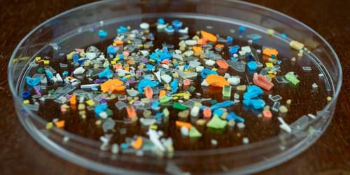
New data on the rotation around both long and short axes of plastic strands may help researchers track and remove microplastics that pollute the ocean.
Pollution from tiny plastic particles (microplastics) increasingly threatens ocean and river ecosystems, and potentially human health, but researchers don’t have a good understanding of how and where these pollutants are transported by flowing waters. Now a research team has observed 1.2-mm-long, 10-µm-wide strands—similar to the most common type of microplastic particles—as they moved in turbulent flows mimicking those in natural environments [1]. The experiments reveal new aspects of their motion, including the rates at which fibers spin around their long axes. The researchers hope that their results will help engineers design structures that can concentrate plastics for easier removal.
Scientists currently have a limited understanding of where microplastics tend to accumulate in the environment, says fluid dynamics expert Alfredo Soldati of the Vienna University of Technology. Where plastics gather depends on natural fluid flows and on the nature of the plastic objects themselves.

Researchers have been delving into the concept of warp drives, theoretically allowing spaceships to surpass the speed of light, using principles from Einstein’s General Relativity.
Physicists have been exploring the theoretical possibility of spaceships driven by compressing the four-dimensional spacetime for decades. Although this so-called “warp drive” originates from the realm of science fiction, it is based on concrete descriptions in general relativity. A new study takes things a step further – simulating the gravitational waves such a drive might emit if it broke down.
Warp Drive Research
Scientists at Argonne National Laboratory have developed a new material that could replace expensive nickel alloys in nuclear reactors.
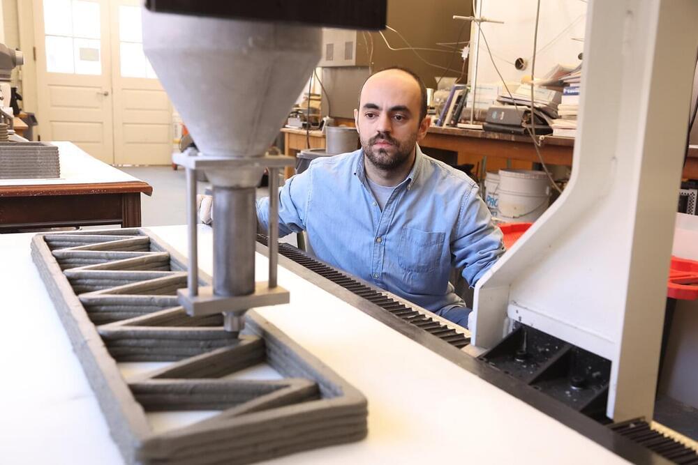
A research team led by engineers at the University of Virginia School of Engineering and Applied Science is the first to explore how an emerging plant-based material, cellulose nanofibrils, could amplify the benefits of 3D-printed concrete technology.
“The improvements we saw on both printability and mechanical measures suggest that incorporating cellulose nanofibrils in commercial printable materials could lead to more resilient and eco-friendly construction practices sooner rather than later,” said Osman E. Ozbulut, a professor in the Department of Civil and Environmental Engineering.
His team’s findings will be published in the September 2024 issue of Cement and Concrete Composites.

MIT physicists and colleagues report new insights into exotic particles key to a form of magnetism that has attracted growing interest because it originates from ultrathin materials only a few atomic layers thick. The work, which could impact future electronics and more, also establishes a new way to study these particles through a powerful instrument at the National Synchrotron Light Source II at Brookhaven National Laboratory.
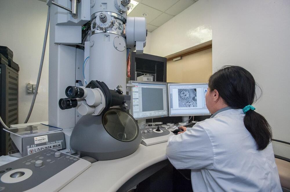
An international team of scientists, led by Trinity College Dublin, has devised an innovative imaging method using state-of-the-art microscopes that significantly reduces the time and radiation required. Their work represents a significant breakthrough that will benefit several disciplines, from materials science to medicine, as the method promises to deliver improved imaging for sensitive materials such as biological tissues that are especially vulnerable to damage.

We asked a professional comedian to deliver some jokes written by artificial intelligence on stage. What happened reveals a lot about just how much machines understand the very human sense of humour.
Karen Hobbs was more nervous than usual before this particular gig. A well-known circuit comedian, she’s accustomed to the UK’s often bruising stand-up comedy scene. It’s eclectic, unpredictable and famously short on pity-laughs. Hobbs has tackled some of the most unforgiving rooms in Britain, from major London theatres to the back rooms of rural pubs. She has even triumphed within the dreaded competition circuit, in which a merciless audience votes in a gladiatorial popularity contest for the funniest gags.
But this Thursday night in late June, above the Covent Garden Social Club bar in Central London, Hobbs was about to attempt something totally new. She would take to the stage equipped not with her usual material, but with a stand-up set written for her by the AI platform ChatGPT. Most daunting of all, she would follow three comedians doing their actual, human material.
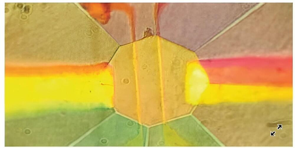
In 1911, Heike Kamerlingh Onnes discovered the first superconductor, metallic mercury when cooled to a critical temperature of 4.2 Kelvin, where it conducts electricity without resistance. Ever since materials scientists have been on a quest to better understand the phenomenon and whether other elements and materials have higher critical temperatures that could make them useful for practical electricity transport, with the holy grail being ambient temperature.
